


 Trouble in Your Tank: Implementing Direct Metallization in Advanced Substrate Packaging
 It’s Only Common Sense: Storytelling That Sells—Stop Pitching, Start Painting Pictures
 The Right Approach: Get Ready for ISO 9001 Version 6


Camouflaging an Optical Chip Rendering it Invisible
November 14, 2017 | Ben-Gurion University of the NegevEstimated reading time: 1 minute
BGU researchers have achieved a breakthrough in manipulating light to theoretically render an object, such as an optical chip, invisible.
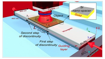
According to the recent study, "Invisibility Cloaking Scheme by Evanescent Distortion on Composite Plasmonic Waveguides with Si Nano-Spacer", published in Nature Scientific Reports, the researchers conceived a new method that deflects and scatters light away from a "cloaking" chip surface so it is not detected.
An operational cloaking chip can be an extension of the basic technologies such as radar-absorbing dark paint used on stealth aircraft, local optical camouflage, surface cooling to minimize electromagnetic infrared emissions, or electromagnetic wave scattering.
Alina 2.jpg"These results open the door to new integrated photonic devices, harnessing electromagnetic fields of light at nanoscale for a variety of applications from on-chip optical devices to all-optical processing," says Dr. Alina Karabchevsky (pictured left), head of BGU's Light-on-a-Chip Group and a member of BGU's Unit of Electro-Optical Engineering and the Ilse Katz Institute for Nanoscale Science and Technology. "We showed that it is possible to bend the light around an object located on the cloak on an optical chip. The light does not interact with the object, thus resulting in the object's invisibility."
The next step is for researchers to overcome the significant challenge of developing a prototype.
Other group researchers who contributed to the study include Yakov Galutin, an MSc student and a member of BGU's Unit of Electro-Optical Engineering and the Ilse Katz Institute for Nanoscale Science and Technology, and Eran Falek, a student in the Department of Electrical and Computer Engineering.
Share on:


Testimonial
"Advertising in PCB007 Magazine has been a great way to showcase our bare board testers to the right audience. The I-Connect007 team makes the process smooth and professional. We’re proud to be featured in such a trusted publication."
Klaus Koziol - atgSuggested Items
HyRel Technologies Showcases Summer Intern Success Through Hands-On Innovation
09/16/2025 | HyRel TechnologiesHyRel Technologies, a global provider of quick turn semiconductor modification solutions, proudly highlights the accomplishments of its two recent summer interns, Danny Hoang and Nisarg Jadav.
ASM Technologies Limited signs MoU with the Guidance, Government of Tamilnadu to Expand Design-Led Manufacturing capabilities for ESDM
09/15/2025 | ASM TechnologiesASM Technologies Limited, a pioneer in Design- Led Manufacturing in the semiconductor and automotive industries, announced signing of Memorandum of Understanding (MoU) with the Guidance, Government of Tamilnadu whereby it will invest Rs. 250 crores in the state to expand its ESDM related Design-Led Manufacturing and precision engineering capacity. ASM Technologies will acquire 5 acres of land from the Government of Tamilnadu to set up a state-of-the-art design facility in Tamil Nadu's growing technology manufacturing ecosystem, providing a strong strategic advantage and long-term benefits for ASM.
Intel Announces Key Leadership Appointments to Accelerate Innovation and Strengthen Execution
09/09/2025 | Intel CorporationIntel Corporation today announced a series of senior leadership appointments that support the company’s strategy to strengthen its core product business, build a trusted foundry, and foster a culture of engineering across the business.
Cadence to Acquire Hexagon’s Design & Engineering Business
09/08/2025 | Cadence Design SystemsCadence announced it has entered into a definitive agreement to acquire the Design & Engineering (D&E) business of Hexagon AB, which includes its MSC Software business—a pioneer in engineering simulation and analysis solutions.
Marcy’s Musings: Continuing to Invent the Future With SEL
08/19/2025 | Marcy LaRont -- Column: Marcy's MusingsTwo years ago, PCB007 Magazine devoted an issue to Schweitzer Engineering Labs (SEL), a new captive greenfield PCB facility in Moscow, Idaho. We highlighted some of the most cutting-edge achievements in facility layout, design, and equipment in the PCB fabrication industry. SEL was a shining example of what was possible, providing insight and inspiration to PCB fabricators looking toward growth and expansion.