


 Trouble in Your Tank: Implementing Direct Metallization in Advanced Substrate Packaging
 It’s Only Common Sense: Storytelling That Sells—Stop Pitching, Start Painting Pictures
 The Right Approach: Get Ready for ISO 9001 Version 6


SLAC X-ray Laser Reveals How Extreme Shocks Deform a Metal’s Atomic Structure
November 15, 2017 | SLAC National Accelerator LaboratoryEstimated reading time: 4 minutes
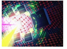
When hit by a powerful shock wave, materials can change their shape – a property known as plasticity – yet keep their lattice-like atomic structure. Now scientists have used the X-ray laser at the Department of Energy’s SLAC National Accelerator Laboratory to see, for the first time, how a material’s atomic structure deforms when shocked by pressures nearly as extreme as the ones at the center of the Earth.
The researchers said this new way of watching plastic deformation as it happens can help study a wide range of phenomena, such as meteor impacts, the effects of bullets and other penetrating projectiles and high-performance ceramics used in armor, as well as how to protect spacecraft from high-speed dust impacts and even how dust clouds form between the stars.
The experiments took place at the Matter in Extreme Condition (MEC) experimental station at SLAC’s Linac Coherent Light Source (LCLS). They were led by Chris Wehrenberg, a physicist at the DOE’s Lawrence Livermore National Laboratory, and described in a recent paper in Nature.
“People have been creating these really high-pressure states for decades, but what they didn't know until MEC came online is exactly how these high pressures change materials – what drives the change and how the material deforms,” said SLAC staff scientist Bob Nagler, a co-author of the report.
“LCLS is so powerful, with so many X-rays in such a short time, that it can interrogate how the material is changing while it is changing. The material changes in just one-tenth of a billionth of a second, and LCLS can deliver enough X-rays to capture information about those changes in a much shorter time that that.”
Elusive Atomic Deformations
The material they studied here was a thin foil made of tantalum, a blue-gray metallic element whose atoms are arranged in cubes. The team used a polycrystalline form of tantalum that is naturally textured so the orientation of these cubes varies little from place to place, making it easier to see certain types of disruptions from the shock.
When this type of crystalline material is squeezed by a powerful shock, it can deform in two distinct ways: twinning, where small regions develop lattice structures that are the mirror images of the ones in surrounding areas, and slip deformation, where a section of the lattice shifts and the displacement spreads, like a propagating crack.
But while these two mechanisms are fundamentally important in plasticity, it’s hard to observe them as a shock is happening. Previous research had studied shocked materials after the fact, as the material recovered, which introduced complications and led to conflicting interpretations.
The Tremendous Shock of a Tiny Recoil
In this experiment, the scientists shocked a piece of tantalum foil with a pulse from an optical laser. This vaporizes a small piece of the foil into a hot plasma that flies away from the surface. The recoil from this tiny plume creates tremendous pressures in the remaining foil – up to 300 gigapascals, which is three million times the atmospheric pressure around us and comparable to the 350-gigapascal pressure at the center of the Earth, Nagler said.
While this was happening, researchers probed the state of the metal with X-ray laser pulses. The pulses are extremely short – only 50 femtoseconds, or millionths of a billionth of a second, long – and like a camera with a very fast shutter speed they can record the metal’s response in great detail.
The X-rays bounce off the metal’s atoms and into a detector, where they create a “diffraction pattern” – a series of bright, concentric rings – that scientists analyze to determine the atomic structure of the sample. X-ray diffraction has been used for decades to discover the structures of materials, biomolecules and other samples and to observe how those structures change, but it’s only recently been used to study plasticity in shock-compressed materials, Wehrenberg said.
And this time the researchers took the technique one step further: They analyzed not just the diffraction patterns, but also how the scattering signals were distributed inside individual diffraction rings and how their distribution changed over time. This deeper level of analysis revealed changes in the tantalum’s lattice orientation, or texture, taking place in about one-tenth of a billionth of a second. It also showed whether the lattice was undergoing twinning or slip over a wide range of shock pressures – right up to the point where the metal melts. The team discovered that as the pressure increased, the dominant type of deformation changed from twinning to slip deformation.
Wehrenberg said the results of this study are directly applicable to Lawrence Livermore’s efforts to model both plasticity and tantalum at the molecular level.
These experiments, he said, “are providing data that the models can be directly compared to for benchmarking or validation. In the future, we plan to coordinate these experimental efforts with related experiments on LLNL’s National Ignition Facility that study plasticity at even higher pressures.”
In addition to LLNL and SLAC, researchers from the University of Oxford, the DOE’s Los Alamos National Laboratory and the University of York contributed to this study. Funding for the work at SLAC came from the DOE Office of Science. LCLS is a DOE Office of Science User Facility.
Share on:


Testimonial
"The I-Connect007 team is outstanding—kind, responsive, and a true marketing partner. Their design team created fresh, eye-catching ads, and their editorial support polished our content to let our brand shine. Thank you all! "
Sweeney Ng - CEE PCBSuggested Items
September 2025 PCB007 Magazine: The Future of Advanced Materials
09/16/2025 | I-Connect007 Editorial TeamMoore’s Law is no more, and the advanced material solutions being developed to grapple with this reality are surprising, stunning, and perhaps a bit daunting. Buckle up for a dive into advanced materials and a glimpse into the next chapters of electronics manufacturing.
I-Connect007 Launches Advanced Electronics Packaging Digest
09/15/2025 | I-Connect007I-Connect007 is pleased to announce the launch of Advanced Electronics Packaging Digest (AEPD), a new monthly digital newsletter dedicated to one of the most critical and rapidly evolving areas of electronics manufacturing: advanced packaging at the interconnect level.
Panasonic Industry will Double the Production Capacity of MEGTRON Multi-layer Circuit Board Materials Over the Next Five Years
09/15/2025 | Panasonic Industry Co., Ltd.Panasonic Industry Co., Ltd., a Panasonic Group company, announced plans for a major expansion of its global production capacity for MEGTRON multi-layer circuit board materials today. The company plans to double its production over the next five years to meet growing demand in the AI server and ICT infrastructure markets.
Trouble in Your Tank: Implementing Direct Metallization in Advanced Substrate Packaging
09/15/2025 | Michael Carano -- Column: Trouble in Your TankDirect metallization systems based on conductive graphite are gaining popularity throughout the world. The environmental and productivity gains achievable with this process are outstanding. Direct metallization reduces the costs of compliance, waste treatment, and legal issues related to chemical exposure. A graphite-based direct plate system has been devised to address these needs.
Fresh PCB Concepts: Designing for Success at the Rigid-flex Transition Area
08/28/2025 | Team NCAB -- Column: Fresh PCB ConceptsRigid-flex PCBs come in all shapes and sizes. Manufacturers typically use fire-retardant, grade 4 (FR-4) materials in the rigid section and flexible polyimide materials in the flex region. Because of the small size, some rigid-flex PCBs, like those for hearing aid devices, are among the most challenging to manufacture. However, regardless of its size, we should not neglect the transition area between the rigid and flexible material.