


 Trouble in Your Tank: Implementing Direct Metallization in Advanced Substrate Packaging
 It’s Only Common Sense: Storytelling That Sells—Stop Pitching, Start Painting Pictures
 The Right Approach: Get Ready for ISO 9001 Version 6


Strain-Free Epitaxy of Germanium Film on Mica
November 20, 2017 | AMERICAN INSTITUTE OF PHYSICSEstimated reading time: 2 minutes
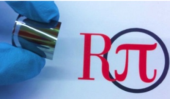
Germanium was the material of choice in the early history of electronic devices, and due to its high charge carrier mobility, it's making a comeback. It's generally grown on expensive single-crystal substrates, adding another challenge to making it sustainably viable for most applications. To address this aspect, researchers demonstrate an epitaxy method that incorporates van der Waals' forces to grow germanium on mica.
Germanium, an elemental semiconductor, was the material of choice in the early history of electronic devices, before it was largely replaced by silicon. But due to its high charge carrier mobility -- higher than silicon by threefold -- the semiconductor is making a comeback.
Germanium (Ge) is generally grown on expensive single-crystal substrates, adding another challenge to making it sustainably viable for most applications. To address this aspect, researchers at Rensselaer Polytechnic Institute in the United States demonstrate an epitaxy method that incorporates van der Waals' forces to grow Ge on mica. Applications could include advanced integrated circuits and high-efficiency solar cells.
"This is the first time strain-free van der Waals epitaxy of an elemental semiconductor has been demonstrated on mica," said Aaron Littlejohn, RPI researcher and co-author of the paper demonstrating the work, published recently in the Journal of Applied Physics, from AIP Publishing.
Growing crystalline film layers on crystalline substrates (called epitaxy) is ubiquitous in semiconductor fabrication. If the film and substrate materials are the same, then the perfectly matched layers form strong chemical bonds for optimal charge carrier mobility.
Layering different materials effectively, however, is a challenge because the crystal lattices typically don't align. To get around this, researchers employed vdW forces, phenomena that are based on the probabilistic nature of electrons, which are not in a fixed position around a nucleus. Rather, they can be anywhere, and the probability that they will be unevenly distributed exists almost all the time. When this happens, there is an induced dipole: a slight positive charge on one side and a slight negative charge opposite. This produces weakly attractive interactions between neutral atoms.
The researchers chose mica as the substrate on which to grow the Ge film because of its atomically smooth surface, which is free of dangling bonds (unpaired valence electrons). This ensured that no chemical bonding would take place during the vdW epitaxy process.
Instead, the materials' interface is held together via weak vdW forces. This allows for the growth of a relaxed film despite the dramatically different crystal structures of the two materials which have a 23 percent difference in atomic spacings. In addition to alleviating the constraints of lattice matching, vdW epitaxy allows the Ge film to be mechanically exfoliated from the mica surface and stand alone as a substrateless film.
"Our Ge film could be used as a thin-film nanomembrane, which could be integrated into electronic devices more easily than nanocrystals or nanowires," Littlejohn said. "It could also serve as the substrate for the subsequent deposition of additional materials for flexible transistors and solar cells, or even wearable optoelectronics."
Geranium films about 80 nanometers thick were grown on millimeter-scale muscovite mica substrates .26 mm thick. By varying the substrate temperature during deposition and annealing in the range of 300-500 degrees Celsius, the researchers found that the crystal lattice stabilizes at about 425 degrees Celsius.
"Previous research implies that elemental semiconductors cannot be epitaxially grown on mica using vdW forces at any elevated temperature, but we have now shown otherwise," Littlejohn said. "With the success of our Ge film grown on mica at a practical temperature, we anticipate that other nonlayered elemental or alloyed materials can be grown on mica via vdW epitaxy."
Share on:


Testimonial
"Our marketing partnership with I-Connect007 is already delivering. Just a day after our press release went live, we received a direct inquiry about our updated products!"
Rachael Temple - AlltematedSuggested Items
September 2025 PCB007 Magazine: The Future of Advanced Materials
09/16/2025 | I-Connect007 Editorial TeamMoore’s Law is no more, and the advanced material solutions being developed to grapple with this reality are surprising, stunning, and perhaps a bit daunting. Buckle up for a dive into advanced materials and a glimpse into the next chapters of electronics manufacturing.
I-Connect007 Launches Advanced Electronics Packaging Digest
09/15/2025 | I-Connect007I-Connect007 is pleased to announce the launch of Advanced Electronics Packaging Digest (AEPD), a new monthly digital newsletter dedicated to one of the most critical and rapidly evolving areas of electronics manufacturing: advanced packaging at the interconnect level.
Panasonic Industry will Double the Production Capacity of MEGTRON Multi-layer Circuit Board Materials Over the Next Five Years
09/15/2025 | Panasonic Industry Co., Ltd.Panasonic Industry Co., Ltd., a Panasonic Group company, announced plans for a major expansion of its global production capacity for MEGTRON multi-layer circuit board materials today. The company plans to double its production over the next five years to meet growing demand in the AI server and ICT infrastructure markets.
Trouble in Your Tank: Implementing Direct Metallization in Advanced Substrate Packaging
09/15/2025 | Michael Carano -- Column: Trouble in Your TankDirect metallization systems based on conductive graphite are gaining popularity throughout the world. The environmental and productivity gains achievable with this process are outstanding. Direct metallization reduces the costs of compliance, waste treatment, and legal issues related to chemical exposure. A graphite-based direct plate system has been devised to address these needs.
Fresh PCB Concepts: Designing for Success at the Rigid-flex Transition Area
08/28/2025 | Team NCAB -- Column: Fresh PCB ConceptsRigid-flex PCBs come in all shapes and sizes. Manufacturers typically use fire-retardant, grade 4 (FR-4) materials in the rigid section and flexible polyimide materials in the flex region. Because of the small size, some rigid-flex PCBs, like those for hearing aid devices, are among the most challenging to manufacture. However, regardless of its size, we should not neglect the transition area between the rigid and flexible material.