


 Trouble in Your Tank: Implementing Direct Metallization in Advanced Substrate Packaging
 It’s Only Common Sense: Storytelling That Sells—Stop Pitching, Start Painting Pictures
 The Right Approach: Get Ready for ISO 9001 Version 6


The Stacked Color Sensor
November 27, 2017 | EMPAEstimated reading time: 3 minutes
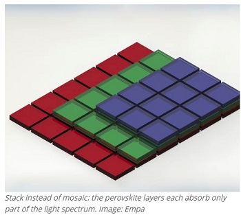
Red-sensitive, blue-sensitive and green-sensitive color sensors stacked on top of each other instead of being lined up in a mosaic pattern – this principle could allow image sensors with unprecedented resolution and sensitivity to light to be created. However, so far, the reality hasn't quite met expectations. Researchers from Empa and ETH Zurich have now developed a sensor prototype that absorbs light almost optimally – and is also cheap to produce.
The human eye has three different types of sensory cells for the perception of color: cells that are respectively sensitive to red, green and blue alternate in the eye and combine their information to create an overall colored image. Image sensors, for example in mobile phone cameras, work in a similar way: blue, green and red sensors alternate in a mosaic-like pattern. Intelligent software algorithms calculate a high-resolution color image from the individual color pixels.
However, the principle also has some inherent limitations: as each individual pixel can only absorb a small part of the light spectrum that hits it, a large part of the light is lost. In addition, the sensors have basically reached the limits of miniaturization, and unwanted image disturbances can occur; these are known as color moiré effects and have to be laboriously removed from the finished image.
Transparent only for certain colors
Researchers have, therefore, been working for a number of years on the idea of stacking the three sensors instead of placing them next to each other. Of course, this requires that the sensors on top let through the light frequencies that they do not absorb to the sensors underneath. At the end of the 1990s, this type of sensor was successfully produced for the first time. It consisted of three stacked silicon layers, each of which absorbed only one color.
This actually resulted in a commercially available image sensor. However, this was not successful on the market because the absorption spectra of the different layers were not distinct enough, so part of the green and red light was absorbed by the blue-sensitive layer. The colors, therefore, blurred and the light sensitivity was thus lower than for ordinary light sensors. In addition, the production of the absorbing silicon layers required a complex and expensive manufacturing process.
Empa researchers have now succeeded in developing a sensor prototype that circumvents these problems. It consists of three different types of perovskites – a semiconducting material that has become increasingly important during the last few years, for example in the development of new solar cells, due to its outstanding electrical properties and good optical absorption capacity (see "Further reading"). Depending on the composition of these perovskites, they can, for example, absorb part of the light spectrum, but remain transparent for the rest of the spectrum. The researchers in Maksym Kovalenko's group at Empa and ETH Zurich used this principle to create a color sensor with a size of just one pixel. The researchers were able to reproduce both simple one-dimensional and more realistic two-dimensional images with an extremely high color fidelity.
Accurate recognition of colors
The advantages of this new approach are clear: the absorption spectra are clearly differentiated and the color recognition is thus much more precise than with silicon. In addition, the absorption coefficients, especially for the light components with higher wavelengths (green and red), are considerably higher in the perovskites than in silicon. As a result, the layers can be made significantly smaller, which in turn allows smaller pixel sizes. This is not crucial in the case of ordinary camera sensors; however, for other analysis technologies, such as spectroscopy, this could permit significantly higher spatial resolution. The perovskites can also be produced using a comparatively cheap process.
However, more work is still needed in order to further develop this prototype into a commercially viable image sensor. Key areas include the miniaturization of pixels and the development of methods for producing an entire matrix of such pixels in one step. According to Kovalenko, this should be possible with existing technologies.
Share on:


Testimonial
"Our marketing partnership with I-Connect007 is already delivering. Just a day after our press release went live, we received a direct inquiry about our updated products!"
Rachael Temple - AlltematedSuggested Items
Kris Moyer Discusses His Emerging Design Technologies Class
09/04/2025 | Marcy LaRont, I-Connect007Kris Moyer, a design instructor for the Global Electronics Association, will be teaching his advanced PCB design class this fall. If you’re ready to level up your design education, you won’t want to miss this interview. The PCB Design for Emerging Design Technologies course is designed to provide the skills necessary to create PCB/PBA designs that require cutting-edge emerging design technologies and comply with all necessary IPC standards, including new standards being developed in this area.
Leadership Change at Koh Young Europe
08/14/2025 | Koh YoungAfter 16 years of leading Koh Young Europe as General Manager, we would like to announce that Harald Eppinger will step down from his executive role.
Driving Innovation: Inner Layer Alignment Methods in PCB Production
08/06/2025 | Kurt Palmer -- Column: Driving InnovationIn PCB manufacturing, precision is a fundamental requirement. Among many complex processes, the accurate registration of inner layers before lamination is one of the most critical. Much like a child's game where rings must be perfectly stacked onto a single pin, PCB manufacturers align multiple conductive and insulating layers to form a cohesive, functional board. This alignment directly affects PCB precision; tighter layer alignment results in smaller "annular rings," superior performance, and higher yields.
From Attraction to Action: Where Marketing Ends and Sales Begins
07/29/2025 | Brittany Martin, I-Connect007Before a PO hits the system, marketing has already done a lot of heavy lifting. Without strategic marketing, the PO might never arrive. At I-Connect007, we have been fortunate to help many companies achieve sales success through marketing. The key to success? Understanding how marketing leads to sales.
Siemens Expands Global Electronics Intelligence Reach and Supplyframe Portfolio with Wevolver Acquisition
04/30/2025 | Siemens Digital Industries SoftwareSiemens Digital Industries Software announced its intention to acquire Wevolver, expanding its audience reach, enhancing the Supplyframe product portfolio, and combining digital marketing and integrated campaign programs that include go-to-market support and content creation.