


 Trouble in Your Tank: Implementing Direct Metallization in Advanced Substrate Packaging
 It’s Only Common Sense: Storytelling That Sells—Stop Pitching, Start Painting Pictures
 The Right Approach: Get Ready for ISO 9001 Version 6


'Magnetoelectric' Material Shows Promise as Memory for Electronics
November 30, 2017 | University of Wisconsin-MadisonEstimated reading time: 2 minutes
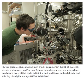
Smartphones and computers wouldn’t be nearly as useful without room for lots of apps, music and videos.
Devices tend to store that information in two ways: through electric fields (think of a flash drive) or through magnetic fields (like a computer’s spinning hard disk). Each method has advantages and disadvantages. However, in the future, our electronics could benefit from the best of each.
“There’s an interesting concept,” says Chang-Beom Eom, the Theodore H. Geballe Professor and Harvey D. Spangler Distinguished Professor of Materials Science and Engineering at the University of Wisconsin–Madison. “Can you cross-couple these two different ways to store information? Could we use an electric field to change the magnetic properties? Then you can have a low-power, multifunctional device. We call this a ‘magnetoelectric’ device.”
In research published recently in the journal Nature Communications, Eom and his collaborators describe not only their unique process for making a high-quality magnetoelectric material, but exactly how and why it works.
Magnetoelectric materials — which have both magnetic and electrical functionalities, or “orders” — already exist. Switching one functionality induces a change in the other.
“It’s called cross-coupling,” says Eom. “Yet, how they cross-couple is not clearly understood.”
Gaining that understanding, he says, requires studying how the magnetic properties change when an electric field is applied. Up to now, this has been difficult due to the complicated structure of most magnetoelectric materials.
In the past, says Eom, people studied magnetoelectric properties using very “complex” materials, or those that lack uniformity. In his approach, Eom simplified not only the research, but the material itself.
Drawing on his expertise in material growth, he developed a unique process, using atomic “steps,” to guide the growth of a homogenous, single-crystal thin film of bismuth ferrite. Atop that, he added cobalt, which is magnetic; on the bottom, he placed an electrode made of strontium ruthenate.
The bismuth ferrite material was important because it made it much easier for Eom to study the fundamental magnetoelectric cross-coupling.
“We found that in our work, because of our single domain, we could actually see what was going on using multiple probing, or imaging, techniques,” he says. “The mechanism is intrinsic. It’s reproducible — and that means you can make a device without any degradation, in a predictable way.”
To image the changing electric and magnetic properties switching in real time, Eom and his colleagues used the powerful synchrotron light sources at Argonne National Laboratory outside Chicago, and in Switzerland and the United Kingdom.
“When you switch it, the electrical field switches the electric polarization. If it’s ‘downward,’ it switches ‘upward,’” he says. “The coupling to the magnetic layer then changes its properties: a magnetoelectric storage device.”
That change in direction enables researchers to take the next steps needed to add programmable integrated circuits — the building blocks that are the foundation of our electronics — to the material.
While the homogenous material enabled Eom to answer important scientific questions about how magnetoelectric cross-coupling happens, it also could enable manufacturers to improve their electronics.
“Now we can design a much more effective, efficient and low-power device,” he says.
Eom’s team includes both theorists and experimentalists, including UW–Madison physics Professor Mark Rzchowski and collaborators at Diamond Light Source in England, Temple University, the University of Oxford, Argonne National Laboratory, Swiss Light Source, Luxembourg Institute of Science and Technology, and Northern Illinois University.
Share on:


Testimonial
"We’re proud to call I-Connect007 a trusted partner. Their innovative approach and industry insight made our podcast collaboration a success by connecting us with the right audience and delivering real results."
Julia McCaffrey - NCAB GroupSuggested Items
MEMS & Imaging Sensors Summit to Spotlight Sensing Revolution for Europe’s Leadership
09/11/2025 | SEMIIndustry experts will gather November 19-20 at the SEMI MEMS & Imaging Sensors Summit 2025 to explore the latest breakthroughs in AI-driven MEMS and imaging optimization, AR/VR technologies, and advanced sensor solutions for critical defence applications.
Direct Imaging System Market Size to Hit $4.30B by 2032, Driven by Increasing Demand for High-Precision PCB Manufacturing
09/11/2025 | Globe NewswireAccording to the SNS Insider, “The Direct Imaging System Market size was valued at $2.21 Billion in 2024 and is projected to reach $4.30 Billion by 2032, growing at a CAGR of 8.68% during 2025-2032.”
I-Connect007’s Editor’s Choice: Five Must-Reads for the Week
07/04/2025 | Marcy LaRont, I-Connect007For our industry, we have seen several bullish market announcements over the past few weeks, including one this week by IDC on the massive growth in the global server market. We’re also closely watching global trade and nearshoring. One good example of successful nearshoring is Rehm Thermal Systems, which celebrates its 10th anniversary in Mexico and the official opening of its new building in Guadalajara.
Driving Innovation: Direct Imaging vs. Conventional Exposure
07/01/2025 | Simon Khesin -- Column: Driving InnovationMy first camera used Kodak film. I even experimented with developing photos in the bathroom, though I usually dropped the film off at a Kodak center and received the prints two weeks later, only to discover that some images were out of focus or poorly framed. Today, every smartphone contains a high-quality camera capable of producing stunning images instantly.
United Electronics Corporation Advances Manufacturing Capabilities with Schmoll MDI-ST Imaging Equipment
06/24/2025 | United Electronics CorporationUnited Electronics Corporation has successfully installed the advanced Schmoll MDI-ST (XL) imaging equipment at their advanced printed circuit board facility. This significant technology investment represents a continued commitment to delivering superior products and maintaining their position as an industry leader in precision PCB manufacturing.