


 It’s Only Common Sense: Stay Curious, My Friends
 The Marketing Minute: AI Is Watching Your Marketing Habits


An atom-thick film of boron could be the first pure two-dimensional material able to emit visible and near-infrared light by activating its plasmons, according to Rice University scientists.
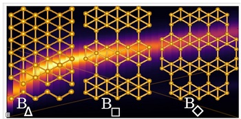
Image caption: Rice University scientists calculate that the atom-thick film of boron known as borophene could be the first pure two-dimensional material naturally able to emit visible and near-infrared light by activating its plasmons. The Rice team tested models of three polymorphs and found that triangular borophene, at left, was capable of emitting visible light, while the other two reached near-infrared. Illustration by Sharmila ShirodkarLong Description
That would make the material known as borophene a candidate for plasmonic and photonic devices like biomolecule sensors, waveguides, nanoscale light harvesters and nanoantennas.
Rice University scientists calculate that the atom-thick film of boron known as borophene could be the first pure two-dimensional material naturally able to emit visible and near-infrared light by activating its plasmons. The Rice team tested models of three polymorphs and found that triangular borophene, at left, was capable of emitting visible light, while the other two reached near-infrared. Illustration by Sharmila Shirodkar
Plasmons are collective excitations of electrons that flow across the surface of metals when triggered by an input of energy, like laser light. Significantly, delivering light to a plasmonic material in one color (determined by the light’s frequency) can prompt the emission of light in another color.
Models by Rice theoretical physicist Boris Yakobson and his colleagues predict that borophene would be the first known 2-D material to do so naturally, without modification.
The lab’s simulations are detailed in a paper by Yakobson with lead authors Yuefei Huang, a graduate student, and Sharmila Shirodkar, a postdoctoral researcher, in the Journal of the American Chemical Society.
Boron is a semiconductor in three dimensions but a metal in 2-D form. That prompted the lab to have a look at its potential for plasmonic manipulation.
“This was kind of anticipated, but we had to do careful work to prove and quantify it,” said Yakobson, whose lab often predicts possible materials that experimentalists later make, like borophene or the boron buckyball. With colleagues Evgeni Penev, an assistant research professor at Rice, and alumnus Zhuhua Zhang, he recently published an extensive review of the state of boron research.
In the new study, the researchers used a computational modeling technique called density functional theory to test plasmonic behavior in three types of free-standing borophene. The material’s baseline crystal structure is a grid of triangles — think graphene but with an extra atom in the middle of each hexagon.
The lab studied models of plain borophene and two polymorphs, solids that incorporate more than one crystalline structure that are formed when some of those middle atoms are removed. Their calculations showed triangular borophene had the widest emission frequencies, including visible light, while the other two reached near-infrared.
“We don’t have enough experimental data to determine which mechanisms contribute how much to the losses in these polymorphs, but we anticipate and include scattering of plasmons against defects and excitation of electrons and holes that lead to their damping,” Shirodkar said.
The researchers said their results present the interesting possibility of manipulating data at subdiffraction wavelengths.
“If you have an optical signal with a wavelength that’s larger than an electronic circuit of a few nanometers, there’s a mismatch,” she said. “Now we can use the signal to excite plasmons in the material that pack the same information (carried by the light) into a much smaller space. It gives us a way to squeeze the signal so that it can go into the electronic circuit.”
“It turns out that’s important because, roughly speaking, it can improve the resolution by 100 times, in some cases,” Yakobson said. “Resolution is limited by wavelength. By using plasmons, you can store information or write into a material at a much higher resolution because of the shrinkage of the wavelength. This could have great benefits for data storage.”
Experimentalists have made borophene only in very small amounts so far and lack methods to transfer the material from the surfaces on which its grown, Yakobson said. Still, there’s plenty for theoretical scientists to study and plenty of progress in the labs.
“One should explore other polymorphs and look for the best one,” Yakobson suggested. “Here, we didn’t. We just considered three, because it’s pretty heavy work — but others need to be screened before we know what is achievable.”
The Army Research Office and the Robert Welch Foundation supported the research. Computational resources were supplied by Rice’s National Science Foundation-supported DAVinCI supercomputer administered by Rice’s Center for Research Computing and procured in partnership with Rice’s Ken Kennedy Institute for Information Technology.
Yakobson is the Karl F. Hasselmann Professor of Materials Science and NanoEngineering and a professor of chemistry.


