


 Trouble in Your Tank: Implementing Direct Metallization in Advanced Substrate Packaging
 It’s Only Common Sense: Storytelling That Sells—Stop Pitching, Start Painting Pictures
 The Right Approach: Get Ready for ISO 9001 Version 6


3-D Printed Objects Connect to WiFi Without Electronics
December 6, 2017 | University of WashingtonEstimated reading time: 3 minutes
Imagine a bottle of laundry detergent that can sense when you’re running low on soap — and automatically connect to the internet to place an order for more.
University of Washington researchers are the first to make this a reality by 3-D printing plastic objects and sensors that can collect useful data and communicate with other WiFi-connected devices entirely on their own.
With CAD models that the team is making available to the public, 3-D printing enthusiasts will be able to create objects out of commercially available plastics that can wirelessly communicate with other smart devices. That could include a battery-free slider that controls music volume, a button that automatically orders more cornflakes from Amazon or a water sensor that sends an alarm to your phone when it detects a leak.
“Our goal was to create something that just comes out of your 3-D printer at home and can send useful information to other devices,” said co-lead author and UW electrical engineering doctoral student Vikram Iyer. “But the big challenge is how do you communicate wirelessly with WiFi using only plastic? That’s something that no one has been able to do before.”
The system is described in a paper presented Nov. 30 at the Association for Computing Machinery’s SIGGRAPH Conference and Exhibition on Computer Graphics and Interactive Techniques in Asia.
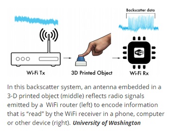
To 3-D print objects that can communicate with commercial WiFi receivers, the team employed backscatter techniques that allow devices to exchange information. In this case, the team replaced some functions normally performed by electrical components with mechanical motion activated by springs, gears, switches and other parts that can be 3-D printed — borrowing from principles that allow battery-free watches to keep time.
Backscatter systems use an antenna to transmit data by reflecting radio signals emitted by a WiFi router or other device. Information embedded in those reflected patterns can be decoded by a WiFi receiver. In this case, the antenna is contained in a 3-D printed object made of conductive printing filament that mixes plastic with copper.
Physical motion — pushing a button, laundry soap flowing out of a bottle, turning a knob, removing a hammer from a weighted tool bench — triggers gears and springs elsewhere in the 3-D printed object that cause a conductive switch to intermittently connect or disconnect with the antenna and change its reflective state.
Information — in the form of 1s and 0s — is encoded by the presence or absence of the tooth on a gear. Energy from a coiled spring drives the gear system, and the width and pattern of gear teeth control how long the backscatter switch makes contact with the antenna, creating patterns of reflected signals that can be decoded by a WiFi receiver.
“As you pour detergent out of a Tide bottle, for instance, the speed at which the gears are turning tells you how much soap is flowing out. The interaction between the 3-D printed switch and antenna wirelessly transmits that data,” said senior author Shyam Gollakota, an associate professor in the Paul G. Allen School of Computer Science & Engineering. “Then the receiver can track how much detergent you have left and when it dips below a certain amount, it can automatically send a message to your Amazon app to order more.”
The team from the UW Networks & Mobile Systems Lab 3-D printed several different tools that were able to sense and send information successfully to other connected devices: a wind meter, a water flow meter and a scale. They also printed a flow meter that was used to track and order laundry soap, and a test tube holder that could be used for either managing inventory or measuring the amount of liquid in each test tube.
They also 3-D printed WiFi input widgets such as buttons, knobs and sliders that can be customized to communicate with other smart devices in the home and enable a rich ecosystem of “talking objects” that can seamlessly sense and interact with their surroundings.
Using a different type of 3-D printing filament that combines plastic with iron, the team also leveraged magnetic properties to invisibly encode static information in 3-D printed objects — which could range from barcode identification for inventory purposes or information about the object that tells a robot how to interact with it.
“It looks like a regular 3-D printed object but there’s invisible information inside that can be read with your smartphone,” said Allen School doctoral student and co-lead author Justin Chan.
Share on:


Testimonial
"Our marketing partnership with I-Connect007 is already delivering. Just a day after our press release went live, we received a direct inquiry about our updated products!"
Rachael Temple - AlltematedSuggested Items
Trouble in Your Tank: Implementing Direct Metallization in Advanced Substrate Packaging
09/15/2025 | Michael Carano -- Column: Trouble in Your TankDirect metallization systems based on conductive graphite are gaining popularity throughout the world. The environmental and productivity gains achievable with this process are outstanding. Direct metallization reduces the costs of compliance, waste treatment, and legal issues related to chemical exposure. A graphite-based direct plate system has been devised to address these needs.
Closing the Loop on PCB Etching Waste
09/09/2025 | Shawn Stone, IECAs the PCB industry continues its push toward greener, more cost-efficient operations, Sigma Engineering’s Mecer System offers a comprehensive solution to two of the industry’s most persistent pain points: etchant consumption and rinse water waste. Designed as a modular, fully automated platform, the Mecer System regenerates spent copper etchants—both alkaline and acidic—and simultaneously recycles rinse water, transforming a traditionally linear chemical process into a closed-loop system.
Driving Innovation: Depth Routing Processes—Achieving Unparalleled Precision in Complex PCBs
09/08/2025 | Kurt Palmer -- Column: Driving InnovationIn PCB manufacturing, the demand for increasingly complex and miniaturized designs continually pushes the boundaries of traditional fabrication methods, including depth routing. Success in these applications demands not only on robust machinery but also sophisticated control functions. PCB manufacturers rely on advanced machine features and process methodologies to meet their precise depth routing goals. Here, I’ll explore some crucial functions that empower manufacturers to master complex depth routing challenges.
Trouble in Your Tank: Minimizing Small-via Defects for High-reliability PCBs
08/27/2025 | Michael Carano -- Column: Trouble in Your TankTo quote the comedian Stephen Wright, “If at first you don’t succeed, then skydiving is not for you.” That can be the battle cry when you find that only small-diameter vias are exhibiting voids. Why are small holes more prone to voids than larger vias when processed through electroless copper? There are several reasons.
The Government Circuit: Navigating New Trade Headwinds and New Partnerships
08/25/2025 | Chris Mitchell -- Column: The Government CircuitAs global trade winds continue to howl, the electronics manufacturing industry finds itself at a critical juncture. After months of warnings, the U.S. Government has implemented a broad array of tariff increases, with fresh duties hitting copper-based products, semiconductors, and imports from many nations. On the positive side, tentative trade agreements with Europe, China, Japan, and other nations are providing at least some clarity and counterbalance.