


 Trouble in Your Tank: Implementing Direct Metallization in Advanced Substrate Packaging
 It’s Only Common Sense: Storytelling That Sells—Stop Pitching, Start Painting Pictures
 The Right Approach: Get Ready for ISO 9001 Version 6


UNIST Researchers Develop Silicon Chip-based Quantum Photonic Devices
December 12, 2017 | UNISTEstimated reading time: 3 minutes
An international team of researchers, affiliated with UNIST has presented a core technology for quantum photonic devices used in quantum information processing. They have proposed combining of quantum dots for generating light and silicon photonic technologies for manipulating light on a single device.
This breakthrough has been led by Professor Je-Hyung Kim in the School of Natural Science at UNIST in collaboration with Professor Edo Waks and a group of researchers at the University of Maryland, United States.
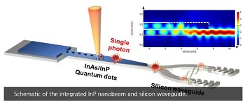
In this study, the research team demonstrated the integration of silicon photonic devices with a solid-state single photon emitter. We use a hybrid approach that combines silicon photonic waveguides with InAs/InP quantum dots that act as efficient sources of single photons at telecom wavelengths spanning the O-band and C-band.
Nano letters 2Schematic of the integrated InP nanobeam and silicon waveguide.
In classical computing, a bit is a single piece of information that can exist in two states – 1 or 0. Quantum computers uses quantum bits that can occupy 0, 1, or a a superposition that can be both at the same time. Although there are several potentially fruitful approaches exist to quantum information processing based on a variety of quantum technologies, including atom, light, and superconducting devices. However, the future of quantum computing, like the quantum state itself, still remains uncertain. Professor Kim focuses on the quantum information processing, using light. This is because quantum bits can be implemented using the polarized state of light, its duration, and the route information, similar to electron spins.
A recently developed quantum light source exhibits the characteristics of quantum physics, including the superposition, quantum entanglement, and no-cloning theorem. This has enabled innovative application technologies, such as quantum simulators, quantum state transfer, and quantum cryptography. However, in order to commercialize the technologies used for the actual quantum information processing technology, it is necessary to perform quantum optics experiments directly on the photonic device. According to the research team, such innovation could be the precursor for quantum circuits, which are expected to play a large role in the future of quantum computers and communication.
“In order to build photon-based integrated quantum optical devices, it is necessary to produce as many quantum light sources as possible in a single chip,” says Professor Kim. “Through this study, we have proposed the basic form of quantum optical devices by producing highly effective quantum light source with quantum dots and creating the pathway to manipulate light with the use of silicon substrates.”
A scanning electron microscope image of the fabricated nanobeam that is suspended by thin tethers that attach it to the bulk substrate.A scanning electron microscope image of the fabricated nanobeam that is suspended by thin tethers that attach it to the bulk substrate.
Quantum dots are ultrafine particles or nanocrystals of a semiconductor material with fiameters in the range of 2 to 10 nanometers (A nanometer is one billionth of a meter). In general, quantum dots take the form of compounds. However, as the size decreases, they begin to exhibit discontinuous energy structure, which results in having similar properties to the light emitted by atoms. Although quantum dots have been used successfully as highly efficient single-photon sources, they had difficulty controlling light.
In the study, the research team demonstrated the integration of silicon photonic devices with a solid-state single photon emitter. Here, they used a hybrid approach that combines silicon photonic waveguides with InAs/InP quantum dots that act as efficient sources of single photons at telecom wavelengths spanning the O-band and C-band. Then, they removed the quantum dots via a pick-and-place procedure with a microprobe tip combined with a focused ion beam and scanning electron microscope. This technique allowed transferring of tapered InP nanobeams containing InAs quantum dots onto a silicon waveguide with nanometer-scale precision.
“This integration opens up the possibility to leverage the highly advanced photonics capabilities developed in silicon to control and route nonclassical light from on-demand single photon sources,” the research team notes. “In addition, the fabricated devices operate at telecom wavelengths and can be electrically driven, which are useful for fiber-based quantum communication.”
The quantum optical device, developed by the research team has successfully transferred the emission from the quantum dots along the silicon photonic circuits with high efficiency. Using this, they also successfully incorporate an on-chip silicon-photonic beamsplitter to perform a Hanbury-Brown and Twiss measurement.
“Our approach could enable integration of precharacterized III–V quantum photonic devices into large-scale photonic structures to enable complex devices composed of many emitters and photons,” says Professor Kim.
Share on:


Testimonial
"In a year when every marketing dollar mattered, I chose to keep I-Connect007 in our 2025 plan. Their commitment to high-quality, insightful content aligns with Koh Young’s values and helps readers navigate a changing industry. "
Brent Fischthal - Koh YoungSuggested Items
Leveraging Chemical Data More Efficiently
07/29/2025 | Lynn L. Bergeson, Bergeson & CampbellSome truths transcend politics, one being that chemical data holds enduring value and is becoming increasingly essential. In the United States, regardless of which party federally controls the levers of power, it’s clear that chemical manufacturers and their customers must develop and curate robust data portfolios for their chemical inventories. The commercial imperatives driving this are undeniable and gaining traction.
2025 ASEAN IT Spending Growth Slows to 5.9% as AI-Powered IT Expansion Encounters Post-Boom Normalization
06/26/2025 | IDCAccording to the IDC Worldwide Black Book: Live Edition, IT spending across ASEAN is projected to grow by 5.9% in 2025 — down from a robust 15.0% in 2024.
Rethinking How Operators Interface With the Line
06/11/2025 | Nolan Johnson, SMT007 MagazineJurgen Schmerler, CEO of WaveOn, reveals how AI and large language models are revolutionizing electronics manufacturing. By integrating AI with machinery, operators can access real-time, multimodal information for troubleshooting and maintenance, significantly reducing training time and enhancing efficiency. He discusses the industry's challenges, the customizable knowledge bases, and the future of proactive maintenance and process control.
Standards: The Roadmap for Your Ideal Data Package
05/29/2025 | Andy Shaughnessy, Design007 MagazineIn this interview, IPC design instructor Kris Moyer explains how standards can help you ensure that your data package has all the information your fabricator and assembler need to build your board the way you designed it, allowing them to use their expertise. As Kris says, even with IPC standards, there’s still an art to conveying the right information in your documentation.
Future-proofing Electronics: ChemFORWARD Works Toward Collaboration for Safer Chemistry
05/19/2025 | Rachel Simon, ChemFORWARDThe electronics industry is facing a critical juncture. As consumer demand for sustainable products rises and regulatory pressures intensify, companies must prioritize the safety of their products and processes. This means not only complying with evolving chemical restrictions but also proactively seeking safer alternatives.