


 Trouble in Your Tank: Implementing Direct Metallization in Advanced Substrate Packaging
 It’s Only Common Sense: Storytelling That Sells—Stop Pitching, Start Painting Pictures
 The Right Approach: Get Ready for ISO 9001 Version 6


Two Holograms in One Surface
December 15, 2017 | CaltechEstimated reading time: 3 minutes
A team at Caltech has figured out a way to encode more than one holographic image in a single surface without any loss of resolution. The engineering feat overturns a long-held assumption that a single surface could only project a single image regardless of the angle of illumination.
The technology hinges on the ability of a carefully engineered surface to reflect light differently depending on the angle at which incoming light strikes that surface.
Holograms are three-dimensional images encoded in two-dimensional surfaces. When the surface is illuminated with a laser, the image seems to pop off the surface and becomes visible. Traditionally, the angle at which laser light strikes the surface has been irrelevant—the same image will be visible regardless. That means that no matter how you illuminate the surface, you will only create one hologram.
Led by Andrei Faraon, assistant professor of applied physics and materials science in the Division of Engineering and Applied Science, the team developed silicon oxide and aluminum surfaces studded with tens of millions of tiny silicon posts, each just hundreds of nanometers tall. (For scale, a strand of human hair is 100,000 nanometers wide.) Each nanopost reflects light differently due to variations in its shape and size, and based on the angle of incoming light.
That last property allows each post to act as a pixel in more than one image: for example, acting as a black pixel if incoming light strikes the surface at 0 degrees and a white pixel if incoming light strikes the surface at 30 degrees.
"Each post can do double duty. This is how we're able to have more than one image encoded in the same surface with no loss of resolution," says Faraon (BS '04), senior author of a paper on the new material published by Physical Review X on December 7.
"Previous attempts to encode two images on a single surface meant arranging pixels for one image side by side with pixels for another image. This is the first time that we're aware of that all of the pixels on a surface have been available for each image," he says.
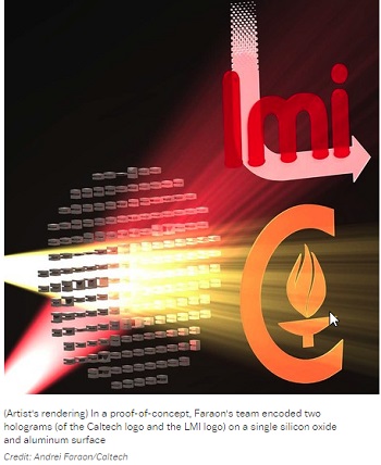
As a proof of concept, Faraon and Caltech graduate student Seyedeh Mahsa Kamali (MS '17) designed and built a surface that when illuminated with a laser straight on (thus, at 0 degrees) projects a hologram of the Caltech logo but when illuminated from an angle of 30 degrees projects a hologram of the logo of the Department of Energy-funded Light-Material Interactions in Energy Conversion Energy Frontier Research Center, of which Faraon is a principal investigator.
The process was labor intensive. "We created a library of nanoposts with information about how each shape reflects light at different angles. Based on that, we assembled the two images simultaneously, pixel by pixel," says Kamali, the first author of the Physical Review X paper.
Theoretically, it would even be possible to encode three or more images on a single surface—though there will be fundamental and practical limits at a certain point. For example, Kamali says that a single degree of difference in the angle of incident light probably cannot be enough to create a new high-quality image. "We are still exploring just how far this technology can go," she says.
Practical applications for the technology include improvements to virtual-reality and augmented-reality headsets. "We're still a long way from seeing this on the market, but it is an important demonstration of what is possible," Faraon says.
The research was published in a paper titled "Angle-Multiplexed Metasurfaces: Encoding Independent Wavefronts in a Single Metasurface under Different Illumination Angles." Faraon and Kamali's coauthors include Caltech graduate students Ehsan Arbabi (MS '17), Yu Horie, and Mohammad Sadegh Faraji-Dana; and Amir Arbabi of the University of Massachusetts Amherst. This work was supported by the Department of Energy, the Defense Advanced Research Projects Agency, and Samsung Electronics.
Written by Robert Perkins
Share on:


Testimonial
"In a year when every marketing dollar mattered, I chose to keep I-Connect007 in our 2025 plan. Their commitment to high-quality, insightful content aligns with Koh Young’s values and helps readers navigate a changing industry. "
Brent Fischthal - Koh YoungSuggested Items
Driving Innovation: Depth Routing Processes—Achieving Unparalleled Precision in Complex PCBs
09/08/2025 | Kurt Palmer -- Column: Driving InnovationIn PCB manufacturing, the demand for increasingly complex and miniaturized designs continually pushes the boundaries of traditional fabrication methods, including depth routing. Success in these applications demands not only on robust machinery but also sophisticated control functions. PCB manufacturers rely on advanced machine features and process methodologies to meet their precise depth routing goals. Here, I’ll explore some crucial functions that empower manufacturers to master complex depth routing challenges.
Polar Instruments Announces Additive Transmission Line Support for Si9000e
08/20/2025 | Polar InstrumentsTransmission lines embedded into the PCB surface are a feature of UHDI constructions. The 2025 fall release of Polar's Si9000e PCB impedance & insertion loss transmission line field solver incorporates eight new single ended, differential and coplanar transmission line structures.
Henniker Plasma Launches Stratus Turnkey Plasma Manufacturing Cell
08/13/2025 | Henniker PlasmaHenniker Plasma, a leading manufacturer of plasma treatment systems, proudly announces the launch of its Stratus Plasma Manufacturing Cell range — a fully integrated, turnkey solution that combines advanced atmospheric plasma surface treatment with robotic automation.
Trouble in Your Tank: Metallizing Flexible Circuit Materials—Mitigating Deposit Stress
08/04/2025 | Michael Carano -- Column: Trouble in Your TankMetallizing materials, such as polyimide used for flexible circuitry and high-reliability multilayer printed wiring boards, provide a significant challenge for process engineers. Conventional electroless copper systems often require pre-treatments with hazardous chemicals or have a small process window to achieve uniform coverage without blistering. It all boils down to enhancing the adhesion of the thin film of electroless copper to these smooth surfaces.
Designers Notebook: Basic PCB Planning Criteria—Establishing Design Constraints
07/22/2025 | Vern Solberg -- Column: Designer's NotebookPrinted circuit board development flows more smoothly when all critical issues are predefined and understood from the start. As a basic planning strategy, the designer must first consider the product performance criteria, then determine the specific industry standards or specifications that the product must meet. Planning also includes a review of all significant issues that may affect the product’s manufacture, performance, reliability, overall quality, and safety.