


 Dan’s Biz Bookshelf: ‘Abundance: How We Build a Better Future’
 Trouble in Your Tank: In Complex Systems, Design Rules Aren’t Optional
 It’s Only Common Sense: The Phone Is Still Your Competitive Advantage


Acoustic Nanodevice Makes Piezoelectrics Sing to a Different Tune
December 20, 2017 | AMERICAN INSTITUTE OF PHYSICSEstimated reading time: 2 minutes
In today’s “internet of things,” devices connect primarily over short ranges at high speeds, an environment in which surface acoustic wave (SAW) devices have shown promise for years, resulting in the shrinking size of your smartphone. To obtain ever faster speeds, however, SAW devices need to operate at higher frequencies, which limits output power and can deteriorate overall performance. A new SAW device looks to provide a path forward for these devices to reach even higher frequencies.
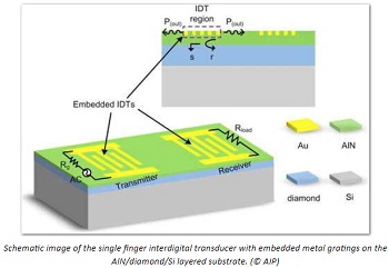
A team of researchers in China has demonstrated a SAW device that can achieve frequencies six times higher than most current devices. With embedded interdigital transducers (IDTs) on a layer of combined aluminum nitride and diamond, the team’s device was also able to boost output significantly. Their results are published this week in Applied Physics Letters ("Enhanced performance of 17.7 GHz SAW devices based on AlN/diamond/Si layered structure with embedded nanotransducer").
“We have found the acoustic field distribution is quite different for the embedded and conventional electrode structures,” said Jinying Zhang, one of the paper’s authors. “Based on the numerical simulation analysis and experimental testing results, we found that the embedded structures bring two benefits: higher frequency and higher output power.”
Surface acoustic wave devices transmit a high-frequency signal by converting electric energy to acoustic energy. This is often done with piezoelectric materials, which are able to change shape in the presence of an electric voltage. IDT electrodes are typically placed on top of piezoelectric materials to perform this conversion.
Ramping up the operational frequency of IDTs -- and the overall signal speed -- has proven difficult. Most current SAW devices top out at a frequency of about 3 gigahertz, Zhang said, but in principle it is possible to make devices that are 10 times faster. Higher frequencies, however, demand more power to overcome the signal loss, and in turn, some features of the IDTs need to be increasingly small. While a 30 GHz device could transmit a signal more quickly, its operational range becomes limited.
“The major challenge is still the fabrication of the IDTs with such small feature sizes,” Zhang said. “Although we made a lot of efforts, there are still small gaps between the side walls of the electrodes and the piezoelectric materials.”
To ensure that the transducers had the proper feature size, Zhang’s team needed a material with a high acoustic velocity, such as diamond. They then coupled diamond, a material that changes its shape very little with electric voltage, with aluminum nitride, a piezoelectric material, and embedded the IDT inside their new SAW device.
The resulting device operated at a frequency of 17.7 GHz and improved power output by 10 percent compared to conventional devices using SAWs.
“The part which surprised us most is that the acoustic field distribution is quite different for the embedded and conventional electrode structures,” Zhang said. “We had no idea at all about it before.”
Zhang said she hopes this research will lead to SAW devices used in monolithic microwave integrated circuits (MMICs), low-cost, high-bandwidth integrated circuits that are seeing use in a variety of forms of high speed communications, such as cell phones.
Share on:


Subscribe
Stay ahead of the technologies shaping the future of electronics with our latest newsletter, Advanced Electronics Packaging Digest. Get expert insights on advanced packaging, materials, and system-level innovation, delivered straight to your inbox.
Subscribe now to stay informed, competitive, and connected.
Suggested Items
High-frequency EMC Noise in DC Circuits
05/29/2025 | Karen Burnham, EMC UnitedEMC isn’t black magic, but it’s easy to understand why it seems that way. When looking at a schematic like that in Figure 1, it looks like you’re only dealing with DC signals all across the board. There’s a 28 VDC input that goes through an EMI filter, then gets converted to 12 VDC power. Except in extremely rare circumstances involving equipment sensitive to magnetostatic fields, DC electricity will never be part of an EMC problem.
Keysight Enabling University of Stuttgart to Advance 6G Integrated Circuits Research
08/10/2023 | Keysight Technologies, Inc.Keysight Technologies, Inc. is enabling the University of Stuttgart to conduct foundational research essential to development of new integrated circuits (IC) for 6G technology with the new Keysight 6G Vector Component Analysis (VCA) solution.
KSG Group Puts Horizontal OSP Line for Organic Surfaces into Operation
07/31/2023 | KSG GroupThe KSG Group has expanded its capacities in the field of organic surface coating by bringing a new wet-chemical horizontal system online.
Mil/Aero Design: Not Just Another High-Rel Board
07/25/2023 | Andy Shaughnessy, Design007 MagazineMeijing Liu, CID+, is a senior PCB designer for Microart Services, an EMS company in Markham, Ontario, Canada. She recently took a six-week military/aerospace PCB design class from IPC’s Kris Moyer, and she was surprised at how much content she was able to absorb in such a short time. I spoke with Meijing and we discussed some of her takeaways from the class, and how it has inspired her to pursue more design education in the future.
MACOM Awarded U.S. Air Force Contract for Advanced Semiconductor Development
07/20/2023 | Business WireMACOM Technology Solutions Inc., a leading supplier of semiconductor products, announced that it has been awarded a contract from the United States Air Force Research Laboratory (“AFRL”) to develop advanced semiconductor process technology related to Gallium Nitride-on-Silicon Carbide (“GaN-on-SiC”).