


 Trouble in Your Tank: Implementing Direct Metallization in Advanced Substrate Packaging
 It’s Only Common Sense: Storytelling That Sells—Stop Pitching, Start Painting Pictures
 The Right Approach: Get Ready for ISO 9001 Version 6


New Technique Allows Rapid Screening for New Types of Solar Cells
December 21, 2017 | MITEstimated reading time: 4 minutes
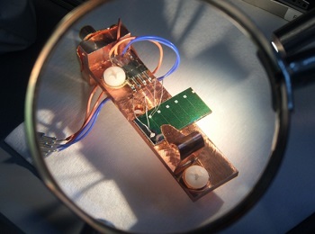
The worldwide quest by researchers to find better, more efficient materials for tomorrow’s solar panels is usually slow and painstaking. Researchers typically must produce lab samples — which are often composed of multiple layers of different materials bonded together — for extensive testing.
Now, a team at MIT and other institutions has come up with a way to bypass such expensive and time-consuming fabrication and testing, allowing for a rapid screening of far more variations than would be practical through the traditional approach.
The new process could not only speed up the search for new formulations, but also do a more accurate job of predicting their performance, explains Rachel Kurchin, an MIT graduate student and co-author of a paper describing the new process that appears this week in the journal Joule. Traditional methods “often require you to make a specialized sample, but that differs from an actual cell and may not be fully representative” of a real solar cell’s performance, she says.
For example, typical testing methods show the behavior of the “majority carriers,” the predominant particles or vacancies whose movement produces an electric current through a material. But in the case of photovoltaic (PV) materials, Kurchin explains, it is actually the minority carriers — those that are far less abundant in the material — that are the limiting factor in a device’s overall efficiency, and those are much more difficult to measure. In addition, typical procedures only measure the flow of current in one set of directions — within the plane of a thin-film material — whereas it’s up-down flow that is actually harnessed in a working solar cell. In many materials, that flow can be “drastically different,” making it critical to understand in order to properly characterize the material, she says.
“Historically, the rate of new materials development is slow — typically 10 to 25 years,” says Tonio Buonassisi, an associate professor of mechanical engineering at MIT and senior author of the paper. “One of the things that makes the process slow is the long time it takes to troubleshoot early-stage prototype devices,” he says. “Performing characterization takes time — sometimes weeks or months — and the measurements do not always have the necessary sensitivity to determine the root cause of any problems.”
So, Buonassisi says, “the bottom line is, if we want to accelerate the pace of new materials development, it is imperative that we figure out faster and more accurate ways to troubleshoot our early-stage materials and prototype devices.” And that’s what the team has now accomplished. They have developed a set of tools that can be used to make accurate, rapid assessments of proposed materials, using a series of relatively simple lab tests combined with computer modeling of the physical properties of the material itself, as well as additional modeling based on a statistical method known as Bayesian inference.
The system involves making a simple test device, then measuring its current output under different levels of illumination and different voltages, to quantify exactly how the performance varies under these changing conditions. These values are then used to refine the statistical model.
“After we acquire many current-voltage measurements [of the sample] at different temperatures and illumination intensities, we need to figure out what combination of materials and interface variables make the best fit with our set of measurements,” Buonassisi explains. “Representing each parameter as a probability distribution allows us to account for experimental uncertainty, and it also allows us to suss out which parameters are covarying.”
The Bayesian inference process allows the estimates of each parameter to be updated based on each new measurement, gradually refining the estimates and homing in ever closer to the precise answer, he says.
In seeking a combination of materials for a particular kind of application, Kurchin says, “we put in all these materials properties and interface properties, and it will tell you what the output will look like.”
The system is simple enough that, even for materials that have been less well-characterized in the lab, “we’re still able to run this without tremendous computer overhead.” And, Kurchin says, making use of the computational tools to screen possible materials will be increasingly useful because “lab equipment has gotten more expensive, and computers have gotten cheaper. This method allows you to minimize your use of complicated lab equipment.”
The basic methodology, Buonassisi says, could be applied to a wide variety of different materials evaluations, not just solar cells — in fact, it may apply to any system that involves a computer model for the output of an experimental measurement. “For example, this approach excels in figuring out which material or interface property might be limiting performance, even for complex stacks of materials like batteries, thermoelectric devices, or composites used in tennis shoes or airplane wings.” And, he adds, “It is especially useful for early-stage research, where many things might be going wrong at once.”
Going forward, he says, “our vision is to link up this fast characterization method with the faster materials and device synthesis methods we’ve developed in our lab.” Ultimately, he says, “I’m very hopeful the combination of high-throughput computing, automation, and machine learning will help us accelerate the rate of novel materials development by more than a factor of five. This could be transformative, bringing the timelines for new materials-science discoveries down from 20 years to about three to five years.”
The research team also included Riley Brandt '11, SM '13, PhD '16; former postdoc Vera Steinmann; MIT graduate student Daniil Kitchaev and visiting professor Gerbrand Ceder, Chris Roat at Google Inc.; and Sergiu Levcenco and Thomas Unold at Hemholz Zentrum in Berlin. The work was supported by a Google Faculty Research Award, the U.S. Department of Energy, and a Total research grant through the MIT Energy Initiative.
Share on:


Testimonial
"In a year when every marketing dollar mattered, I chose to keep I-Connect007 in our 2025 plan. Their commitment to high-quality, insightful content aligns with Koh Young’s values and helps readers navigate a changing industry. "
Brent Fischthal - Koh YoungSuggested Items
Meet the Author Podcast: Martyn Gaudion Unpacks the Secrets of High-Speed PCB Design
07/16/2025 | I-Connect007In this special Meet the Author episode of the On the Line with… podcast, Nolan Johnson sits down with Martyn Gaudion, signal integrity expert, managing director of Polar Instruments, and three-time author in I-Connect007’s popular The Printed Circuit Designer’s Guide to... series.
Intervala Hosts Employee Car and Motorcycle Show, Benefit Nonprofits
08/27/2024 | IntervalaIntervala hosted an employee car and motorcycle show, aptly named the Vala-Cruise and it was a roaring success! Employees had the chance to show off their prized wheels, and it was incredible to see the variety and passion on display.
KIC Honored with IPC Recognition for 25 Years of Membership and Contributions to Electronics Manufacturing Industry
06/24/2024 | KICKIC, a renowned pioneer in thermal process and temperature measurement solutions for electronics manufacturing, is proud to announce that it has been recognized by IPC for 25 years of membership and significant contributions to electronics manufacturing.
Boeing Starliner Spacecraft Completes Successful Crewed Docking with International Space Station
06/07/2024 | BoeingNASA astronauts Barry "Butch" Wilmore and Sunita "Suni" Williams successfully docked Boeing's Starliner spacecraft to the International Space Station (ISS), about 26 hours after launching from Cape Canaveral Space Force Station.
KIC’s Miles Moreau to Present Profiling Basics and Best Practices at SMTA Wisconsin Chapter PCBA Profile Workshop
01/25/2024 | KICKIC, a renowned pioneer in thermal process and temperature measurement solutions for electronics manufacturing, announces that Miles Moreau, General Manager, will be a featured speaker at the SMTA Wisconsin Chapter In-Person PCBA Profile Workshop.