


 Trouble in Your Tank: Implementing Direct Metallization in Advanced Substrate Packaging
 It’s Only Common Sense: Storytelling That Sells—Stop Pitching, Start Painting Pictures
 The Right Approach: Get Ready for ISO 9001 Version 6


Thermoelectric Power Generation at Room Temperature: Coming Soon?
December 27, 2017 | Osaka UniversityEstimated reading time: 2 minutes
Thermoelectric (TE) materials could play a key role in future technologies. Although the applications of these remarkable compounds have long been explored, they are mostly limited to high-temperature devices.
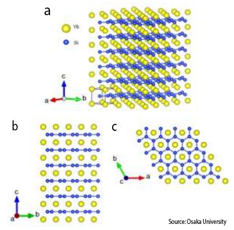
Figure 1. (a) Three-dimensional crystal structure of YbSi2, (b) view along the a-axis, and (c) along the c-axis.
Recently, researchers at Osaka University, in collaboration with Hitachi, Ltd., developed a new TE material with an improved power factor at room temperature. Their study, published in Physica Status Solidi RRL, could help bring these materials out of the high-temperature niche and into the mainstream.
TE materials display the thermoelectric effect: apply heat on one side, and an electric current starts to flow. Conversely, run an external current through the device, and a temperature gradient forms; i.e., one side becomes hotter than the other. By interconverting heat and electricity, TE materials can be used as either power generators (given a heat source) or refrigerators (given a power supply).
The ideal TE material combines high electrical conductivity, allowing the current to flow, with low thermal conductivity, which prevents the temperature gradient from evening out. The power generation performance mainly depends on the “power factor,” which is proportional to both electrical conductivity and a term called the Seebeck coefficient.
“Unfortunately, most TE materials are often based on rare or toxic elements,” according to study co-author Sora-at Tanusilp. “To address this, we combined silicon – which is common in TE materials – with ytterbium, to create ytterbium silicide [YbSi2]. We chose ytterbium over other metals for several reasons. First, its compounds are good electrical conductors. Second, YbSi2 is non-toxic. Moreover, this compound has a specific property called valence fluctuation that make it a good TE material at low temperatures.”
The first advantage of YbSi2 is that the Yb atoms occupy a mixture of valence states, both +2 and +3. This fluctuation, also known as Kondo resonance, increases the Seebeck coefficient with keeping metal-like high electrical conductivity at low temperature, and therefore the power factor.
Second, YbSi2 has an unusual layered structure. While the Yb atoms occupy crystal planes similar to pure Yb metal, the Si atoms form hexagonal sheets between those planes, resembling the carbon sheets in graphite. This blocks the conduction of heat through the material, and therefore keeps the thermal conductivity down, preserving the temperature gradient. The researchers believe that heat conduction is further suppressed by controlling the structure in nanoscale and traces of impurities and other defects.
The result is an encouragingly high power factor of 2.2 mWm-1K-2 at room temperature. This is competitive with conventional TE materials based on bismuth telluride. As corresponding author of this study Ken Kurosaki explains, “The use of Yb shows we can reconcile the conflicting needs of TE materials through carefully selecting the right metals. Room-temperature TEs, with moderate power, can be seen as complementary to the conventional high-temperature, high-power devices. This could help unlock the benefits of TE in everyday technology.”
Share on:


Testimonial
"The I-Connect007 team is outstanding—kind, responsive, and a true marketing partner. Their design team created fresh, eye-catching ads, and their editorial support polished our content to let our brand shine. Thank you all! "
Sweeney Ng - CEE PCBSuggested Items
September 2025 PCB007 Magazine: The Future of Advanced Materials
09/16/2025 | I-Connect007 Editorial TeamMoore’s Law is no more, and the advanced material solutions being developed to grapple with this reality are surprising, stunning, and perhaps a bit daunting. Buckle up for a dive into advanced materials and a glimpse into the next chapters of electronics manufacturing.
I-Connect007 Launches Advanced Electronics Packaging Digest
09/15/2025 | I-Connect007I-Connect007 is pleased to announce the launch of Advanced Electronics Packaging Digest (AEPD), a new monthly digital newsletter dedicated to one of the most critical and rapidly evolving areas of electronics manufacturing: advanced packaging at the interconnect level.
Panasonic Industry will Double the Production Capacity of MEGTRON Multi-layer Circuit Board Materials Over the Next Five Years
09/15/2025 | Panasonic Industry Co., Ltd.Panasonic Industry Co., Ltd., a Panasonic Group company, announced plans for a major expansion of its global production capacity for MEGTRON multi-layer circuit board materials today. The company plans to double its production over the next five years to meet growing demand in the AI server and ICT infrastructure markets.
Trouble in Your Tank: Implementing Direct Metallization in Advanced Substrate Packaging
09/15/2025 | Michael Carano -- Column: Trouble in Your TankDirect metallization systems based on conductive graphite are gaining popularity throughout the world. The environmental and productivity gains achievable with this process are outstanding. Direct metallization reduces the costs of compliance, waste treatment, and legal issues related to chemical exposure. A graphite-based direct plate system has been devised to address these needs.
Fresh PCB Concepts: Designing for Success at the Rigid-flex Transition Area
08/28/2025 | Team NCAB -- Column: Fresh PCB ConceptsRigid-flex PCBs come in all shapes and sizes. Manufacturers typically use fire-retardant, grade 4 (FR-4) materials in the rigid section and flexible polyimide materials in the flex region. Because of the small size, some rigid-flex PCBs, like those for hearing aid devices, are among the most challenging to manufacture. However, regardless of its size, we should not neglect the transition area between the rigid and flexible material.