Orbotech Presented Ultra Dimension Series at HKPCA 2017
December 28, 2017 | OrbotechEstimated reading time: 3 minutes

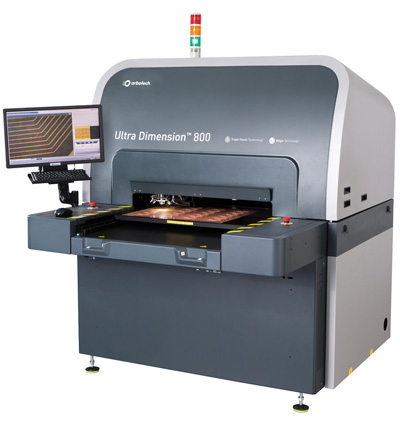
Orbotech Ltd. presented its new Ultra Dimension AOI (Automated Optical Inspection) series at the recent PCB industry HKPCA 2017 show in Shenzhen, China. The Ultra Dimension was showcased in a model AOI room along with the Precise 800 AOS (Automated Optical Shaping), remote multi-image verification (RMIV) station and Orbotech Data Server, attracting approximately 500 visitors during the three days of the show. In addition, Orbotech also presented its Nuvogo Fine Direct Imaging solution, as well as Orbotech Smart Factory solution for Industry 4.0 and Frontline’s CAM and Engineering solutions.
Designed to meet the rigorous demands of advanced PCB manufacturing using SLP/mSAP (substrate-like PCB/modified semi-additive process), the innovative Ultra Dimension is the first AOI solution to integrate four leading systems into one. The solution, which includes pattern inspection, laser via inspection, Remote Multi-Image Verification and 2D metrology, signifies a revolution in the AOI room workflow and enables manufacturers to increase quality and yield while dramatically reducing their overall total cost of ownership (TCO).
“Orbotech’s new AOI room concept together with our new Ultra Dimension, attracted positive attention at HKPCA,” commented Hadar Himmelman, President of Orbotech Pacific. “The feedback that we received on our new 4-in-1 AOI solution is that it represents a real revolution in the AOI room workflow. Together with its ability to reduce TCO, the Ultra Dimension meets our customers’ needs as the market becomes more sophisticated.
”Ultra Dimension’s combination of high precision and high quality pattern inspection and laser via (LV) inspection in a single scan is powered by Orbotech’s proprietary Triple Vision Technology and Magic Technology. By using varied light settings and three different types of images, these technologies enable Ultra Dimension to improve detection capabilities significantly, reduce false alarms and decrease inspection set-up time. This, in turn, allows manufacturers of advanced PCBs using SLP/mSAP (substrate-like PCB/modified semi-additive process) the flexibility to inspect a variety of applications and materials, and eliminates the need to use inspection masks which can cause defects to be overlooked.
Orbotech’s 2D metrology automatically measures both top and bottom conductor widths for lines and pads of a wide variety of shapes, enabling the higher accuracy and impedance control necessary for SLP/mSAP as well as advanced HDI applications.
Orbotech’s Remote Multi-Image Verification (RMIV) enables the remote verification of multiple image defects, which are automatically and simultaneously acquired during the inspection process. Orbotech’s unique multi-image technology enables operators to accurately differentiate between real and false defects, which are then sent to offline RMIV stations. Ultra Dimension with RMIV also reduces the number of verification stations required, thereby freeing up valuable floor space in the AOI room and allowing manufacturers to cut their overall labor and operational costs significantly.
For the second year running, Orbotech won a prize for booth design from the HKPCA Association. The prize was awarded at a gala dinner event during the show.
About Orbotech Ltd.
Orbotech Ltd. is a leading global supplier of yield-enhancing and process-enabling solutions for the manufacture of electronics products. Orbotech provides cutting-edge solutions for use in the manufacture of printed circuit boards (PCBs), flat panel displays (FPDs), and semiconductor devices (SDs), designed to enable the production of innovative, next-generation electronic products and improve the cost effectiveness of existing and future electronics production processes. Orbotech’s core business lies in enabling electronic device manufacturers to inspect and understand PCBs and FPDs and to verify their quality (‘reading’); pattern the desired electronic circuitry on the relevant substrate and perform three-dimensional shaping of metalized circuits on multiple surfaces (‘writing’); and utilize advanced vacuum deposition and etching processes in SD and semiconductor manufacturing (‘connecting’). Orbotech refers to this ‘reading’, ‘writing’ and ‘connecting’ as enabling the ‘Language of Electronics’. For more information, click here.
Suggested Items
I-Connect007 Editor’s Choice: Five Must-Reads for the Week
05/30/2025 | Andy Shaughnessy, Design007I don’t have a scorecard, but I do have a weekly wrap-up of must-reads that I think deserve another “bite of the apple,” so to speak. IPC’s Rich Cappetto shares his perspective on everything from tariffs to the CHIPS Act. Columnist Josh Casper discusses the use of AI in 3D AOI systems and the immediate benefits that AI can bring about. Columnist Anaya Vardya explains how technologies like AI can improve our customer service, as well as our manufacturing processes.
Smart Automation: AI—Revolutionizing Inspection in Electronics Manufacturing
05/27/2025 | Josh Casper -- Column: Smart AutomationArtificial Intelligence (AI) is rapidly becoming a staple in our personal and professional lives. In electronics manufacturing, integrating AI to combat common inefficiencies and to contextualize data will open new doors into how we supplement our traditional processes. In some specific areas of the electronics manufacturing process, integration of AI on the factory floor is already having a tremendous effect. One such area is PCBA inspection, particularly 3D automated optical inspection (AOI) systems.
I-Connect007 Editor’s Choice: Five Must-Reads for the Week
05/23/2025 | Marcy LaRont, I-Connect007In the electronics manufacturing industry, the global PCB market is estimated to reach $86.5 billion by 2029, a 5.9% annual growth, per IPC’s Global Market Forecast, and the global new cycle is still being dominated by U.S. news. This week, we are talking about the status of the CHIPS Act and what the new tax and incentives bill does and does not include. We also take a minute for some marketing wisdom to shed light in a challenging and noisy market environment.
Hunting for Clues: Feng Xue Solving Circuit Board 'Crimes' With AOI Standard
05/08/2025 | Linda Stepanich, IPCWhen residents in sleepy English villages needed a top-tier detective to solve a murder, they called on Belgian super-sleuth Hercule Poirot, author Agatha Christie’s fictional detective famous for using his “little grey cells” to solve crimes. In the same way, IPC standards development committees, when creating a standard to detect defects in circuit boards using Automated Optical Inspection (AOI), call on IPC A-Team, Hercule.
Real Time with... IPC APEX EXPO 2025: TRI Innovation—Transforming Semiconductor Inspection with AI Technology
04/25/2025 | Real Time with...IPC APEX EXPONolan Johnson talks with David Chiu, USA Sales Manager for TRI Innovation. TRI uses advanced technology to tackle challenges in inspecting tiny components. Their AI programming reduces coding time by 75%, enhancing efficiency in inspections. Collaborating with Nvidia, TRI integrates GPU technology to improve product development and encourages customers to share data for better AI performance.
Copyright © 2025 I-Connect007 | IPC Publishing Group Inc. All rights reserved.
Log in