


 Trouble in Your Tank: Implementing Direct Metallization in Advanced Substrate Packaging
 It’s Only Common Sense: Storytelling That Sells—Stop Pitching, Start Painting Pictures
 The Right Approach: Get Ready for ISO 9001 Version 6


Steering Electrical Current With Spinning Light
December 28, 2017 | University of MinnesotaEstimated reading time: 4 minutes
Light can generate an electrical current in semiconductor materials. This is how solar cells generate electricity from sunlight and how smart phone cameras can take photographs. To collect the generated electrical current, called photocurrent, an electric voltage is needed to force the current to flow in only one direction.
In new research, scientists at the University of Minnesota used a first-of-its-kind device to demonstrate a way to control the direction of the photocurrent without deploying an electric voltage. The new study was recently published in the scientific journal Nature Communications.
The study reveals that control is effected by the direction in which the particles of light, called photons, are spinning -- clockwise or counterclockwise. The photocurrent generated by the spinning light is also spin-polarized, which means there are more electrons with spin in one direction than in the other. This new device holds significant potential for use in the next generation of microelectronics using electron spin as the fundamental unit of information. It could also be used for energy efficient optical communication in data centers.
"The observed effect is very strong and robust in our devices, even at room temperature and in open air," said Mo Li, a University of Minnesota electrical and computer engineering associate professor and a lead author of the study. "Therefore, the device we demonstrate has great potential for being implemented in next-generation computation and communication systems."
Optical spin and topological insulators
Light is a form of electromagnetic wave. The way the electric field oscillates, either in a straight line or rotating, is called polarization. (Your polarized sunglasses block part of the unpleasant reflected light that is polarized along a straight line.) In circularly polarized light, the electric field can spin in the clockwise or counterclockwise direction. In such a state, the particle of light (photon) is said to have positive or negative optical spin angular momentum. This optical spin is analogous to the spin of electrons, and endows magnetic properties to materials.
Recently, a new category of materials, called topological insulators (TI), was discovered to have an intriguing property not found in common semiconductor materials. Imagine a road on which red cars only drive on the left lane, and blue cars only in the right lane. Similarly, on the surface of a TI, the electrons with their spins pointing one way always flow in one direction. This effect is called spin-momentum locking -- the spin of the electrons is locked in the direction they travel.
Interestingly, shining a circularly polarized light on a TI can free electrons from its inside to flow on its surface in a selective way, for example, clockwise light for spin-up electrons and counterclockwise for spin-down electrons. Because of this effect, the generated photocurrent on the surface of the TI material spontaneously flows in one direction, requiring no electric voltage. This particular feature is significant for controlling the direction of a photocurrent. Because most of the electrons in this current have their spins pointing in a single direction, this current is spin-polarized.
Controlling direction and polarization
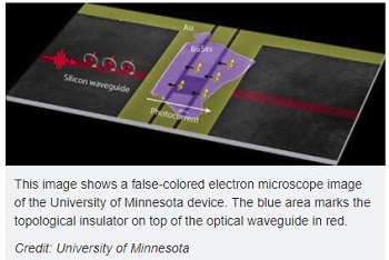
To fabricate their unique device that can change the direction of a photocurrent without the use of an electric voltage, the University's research team integrated a thin film of a TI material, bismuth selenide, on an optical waveguide made of silicon. Light flows through the waveguide (a tiny wire measuring 1.5 microns wide and 0.22 micron high) just like electrical current flows through a copper wire. Because light is tightly squeezed in the waveguide, it tends to be circularly polarized along a direction normal to the direction in which it flows. This is akin to the spin-momentum locking effect of the electrons in a TI material.
The scientists supposed that integrating a TI material with the optical waveguide will induce strong coupling between the light in the waveguide and the electrons in the TI material, both having the same, intriguing spin-momentum locking effect. The coupling will result in a unique optoelectronic effect -- light flowing along one direction in the waveguide generates an electrical current flowing in the same direction with electron spin polarized.
Reversing the light direction reverses both the direction of the current and its spin polarization. And this is exactly what the team observed in their devices. Other possible causes of the observed effect, such as heat generated by the light, have been ruled out through careful experiments.
Future prospects
The outcome of the research is exciting for the researchers. It bears enormous potential for possible applications.
"Our devices generate a spin-polarized current flowing on the surface of a topological insulator. They can be used as a current source for spintronic devices, which use electron spin to transmit and process information with very low energy cost," said Li He, a University of Minnesota physics graduate student and an author of the paper.
"Our research bridges two important fields of nanotechnology: spintronics and nanophotonics. It is fully integrated with a silicon photonic circuit that can be manufactured on a large scale and has already been widely used in optical communication in data centers," He added.
This research was funded by the Center for Spintronic Materials, Interfaces and Novel Architectures (C-SPIN) at the University of Minnesota, a Semiconductor Research Corporation program sponsored by the Microelectronics Advanced Research Corp. (MARCO) and the Defense Advanced Research Projects Agency (DARPA), and the National Science Foundation (NSF).
Parts of this research were carried out in the University of Minnesota Nanofabrication Center which receives partial support from NSF through National Nanotechnology Coordinated Infrastructure (NNCI) program, and the Characterization Facility which is a member of the NSF-funded Materials Research Facilities Network via the University of Minnesota Materials Research Science and Engineering Center (MRSEC) program. Li He received a Doctoral Dissertation Fellowship provided by the University of Minnesota Graduate School that supported his work.
Share on:


Testimonial
"Advertising in PCB007 Magazine has been a great way to showcase our bare board testers to the right audience. The I-Connect007 team makes the process smooth and professional. We’re proud to be featured in such a trusted publication."
Klaus Koziol - atgSuggested Items
Trouble in Your Tank: Implementing Direct Metallization in Advanced Substrate Packaging
09/15/2025 | Michael Carano -- Column: Trouble in Your TankDirect metallization systems based on conductive graphite are gaining popularity throughout the world. The environmental and productivity gains achievable with this process are outstanding. Direct metallization reduces the costs of compliance, waste treatment, and legal issues related to chemical exposure. A graphite-based direct plate system has been devised to address these needs.
Closing the Loop on PCB Etching Waste
09/09/2025 | Shawn Stone, IECAs the PCB industry continues its push toward greener, more cost-efficient operations, Sigma Engineering’s Mecer System offers a comprehensive solution to two of the industry’s most persistent pain points: etchant consumption and rinse water waste. Designed as a modular, fully automated platform, the Mecer System regenerates spent copper etchants—both alkaline and acidic—and simultaneously recycles rinse water, transforming a traditionally linear chemical process into a closed-loop system.
Driving Innovation: Depth Routing Processes—Achieving Unparalleled Precision in Complex PCBs
09/08/2025 | Kurt Palmer -- Column: Driving InnovationIn PCB manufacturing, the demand for increasingly complex and miniaturized designs continually pushes the boundaries of traditional fabrication methods, including depth routing. Success in these applications demands not only on robust machinery but also sophisticated control functions. PCB manufacturers rely on advanced machine features and process methodologies to meet their precise depth routing goals. Here, I’ll explore some crucial functions that empower manufacturers to master complex depth routing challenges.
Trouble in Your Tank: Minimizing Small-via Defects for High-reliability PCBs
08/27/2025 | Michael Carano -- Column: Trouble in Your TankTo quote the comedian Stephen Wright, “If at first you don’t succeed, then skydiving is not for you.” That can be the battle cry when you find that only small-diameter vias are exhibiting voids. Why are small holes more prone to voids than larger vias when processed through electroless copper? There are several reasons.
The Government Circuit: Navigating New Trade Headwinds and New Partnerships
08/25/2025 | Chris Mitchell -- Column: The Government CircuitAs global trade winds continue to howl, the electronics manufacturing industry finds itself at a critical juncture. After months of warnings, the U.S. Government has implemented a broad array of tariff increases, with fresh duties hitting copper-based products, semiconductors, and imports from many nations. On the positive side, tentative trade agreements with Europe, China, Japan, and other nations are providing at least some clarity and counterbalance.