


 Trouble in Your Tank: Implementing Direct Metallization in Advanced Substrate Packaging
 It’s Only Common Sense: Storytelling That Sells—Stop Pitching, Start Painting Pictures
 The Right Approach: Get Ready for ISO 9001 Version 6


Viewing Atomic Structures of Dopant Atoms in 3-D Relating to Electrical Activity in a Semiconductor
December 29, 2017 | Tokyo Institute of TechnologyEstimated reading time: 3 minutes
Scientists at Tokyo Institute of Technology (Tokyo Tech) and their research team involving researchers of JASRI, Osaka University, Nagoya Institute of Technology, and Nara Institute of Science and Technology have just developed a novel approach to determine and visualize the three-dimensional (3D) structure of individual dopant atoms using SPring-8. The technique will help improve the current understanding of the atomic structures of dopants in semiconductors correlated with their electrical activity and thus help support the development of new manufacturing processes for high-performance devices.
Using a combination of spectro-photoelectron holography, electrical property measurements, and first-principles dynamics simulations, the 3D atomic structures of dopant impurities in a semiconductor crystal were successfully revealed. The need for a better understanding of the atomic structures of dopants in semiconductors had been long felt, mainly because the current limitations on active dopant concentrations result from the deactivation of excess dopant atoms by the formation of various types of clusters and other defect structures.
The search for techniques to electrically activate the dopant impurities in semiconductors with high efficiency and/or at high concentrations have always been an essential aspect of semiconductor device technology. However, despite various successful developments, the achievable maximum concentration of active dopants remains limited. Given the impact of the dopant atomic structures in this process, these structures had been previously investigated using both theoretical and experimental approaches. However, direct observation of the 3D structures of the dopant atomic arrangements had hitherto been difficult to achieve.
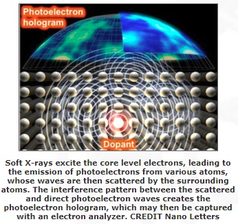
In this study, Kazuo Tsutsui at Tokyo Tech and colleagues involving researchers at JASRI, Osaka University, Nagoya Institute of Technology, and Nara Institute of Science and Technology developed spectro-photoelectron holography using SPring-8, and leveraged the capabilities of photoelectron holography in determining the concentrations of dopants at different sites, based on the peak intensities of the photoelectron spectrum, and classified electrically active / inactive atomic sites. These structures directly related with the density of carriers. In this approach, soft X-ray excitation of the core level electrons leads to the emission of photoelectrons from various atoms, whose waves are then scattered by the surrounding atoms. The resulting interference pattern creates the photoelectron hologram, which may then be captured with an electron analyzer. The photoelectron spectra acquired in this manner contain information from more than one atomic site. Therefore, peak fitting is performed to obtain the photoelectron hologram of individual atomic sites. The combination of this technique with first-principles simulations allows the successful estimation of the 3D structure of the dopant atoms, and the assessment of their different chemical bonding states. The method was used to estimate the 3D structures of arsenic atoms doped onto a silicon surface. The obtained results fully demonstrated the power of the proposed method and allowed confirmation of several previous results.
This work demonstrates the potential of spectro-photoelectron holography for the analysis of impurities in semiconductors. This technique allows analyses that are difficult to perform with conventional approaches and should therefore be useful in the development of improved doping techniques and, ultimately, in supporting the manufacture of high-performance devices.
About Tokyo Institute of Technology
Tokyo Institute of Technology stands at the forefront of research and higher education as the leading university for science and technology in Japan. Tokyo Tech researchers excel in a variety of fields, such as material science, biology, computer science and physics. Founded in 1881, Tokyo Tech has grown to host 10,000 undergraduate and graduate students who become principled leaders of their fields and some of the most sought-after scientists and engineers at top companies. Embodying the Japanese philosophy of "monotsukuri," meaning technical ingenuity and innovation, the Tokyo Tech community strives to make significant contributions to society through high-impact research.
Share on:


Testimonial
"In a year when every marketing dollar mattered, I chose to keep I-Connect007 in our 2025 plan. Their commitment to high-quality, insightful content aligns with Koh Young’s values and helps readers navigate a changing industry. "
Brent Fischthal - Koh YoungSuggested Items
Altair, Wichita State University’s NIAR Sign MoU to Accelerate Aerospace Innovation
09/16/2025 | AltairAltair, a global leader in computational intelligence, and Wichita State University’s (WSU) National Institute for Aviation Research (NIAR), one of the world’s leading aerospace research institutions, have signed a memorandum of understanding (MoU) to advance innovation across the aerospace and defense industries.
AI-Powered Wearables Transform How Consumers Interact with Everyday Technology
09/15/2025 | PR NewswireThe global demand for AI-driven, touchless wearable technologies is accelerating as consumers seek more natural, seamless and intuitive ways to interact with their devices. Traditional touch screens and voice assistants, while effective, are increasingly viewed as limiting in a world where multitasking, mobility and efficiency are key. As industries from consumer electronics to augmented reality and enterprise computing embrace the possibilities of gesture-based control, the market for neural interfaces is rapidly expanding
Hanwha Aerospace to Collaborate with BAE Systems on Advanced Anti-jamming GPS for Guided Missiles
09/15/2025 | HanwhaHanwha Aerospace has signed a contract with BAE Systems to integrate next-generation, anti-jamming Global Positioning System (GPS) technology into Hanwha Aerospace’s Deep Strike Capability precision-guided weapon system.
United Electronics Corporation Unveils Revolutionary CIMS Galaxy 30 Automated Optical Inspection System
09/11/2025 | United Electronics CorporationUnited Electronics Corporation (UEC) today announced the launch of its new groundbreaking CIMS Galaxy 30 Automated Optical Inspection (AOI) machine, setting a new industry standard for precision electronics manufacturing quality control. The Galaxy 30, developed and manufactured by CIMS, represents a significant leap forward in inspection technology, delivering exceptional speed improvements and introducing cutting-edge artificial intelligence capabilities.
Intel Announces Key Leadership Appointments to Accelerate Innovation and Strengthen Execution
09/09/2025 | Intel CorporationIntel Corporation today announced a series of senior leadership appointments that support the company’s strategy to strengthen its core product business, build a trusted foundry, and foster a culture of engineering across the business.