


 Trouble in Your Tank: Implementing Direct Metallization in Advanced Substrate Packaging
 It’s Only Common Sense: Storytelling That Sells—Stop Pitching, Start Painting Pictures
 The Right Approach: Get Ready for ISO 9001 Version 6


Laser Evaporation Technology to Create New Solar Materials
January 4, 2018 | Duke UniversityEstimated reading time: 3 minutes
Materials scientists at Duke University have developed a method to create hybrid thin-film materials that would otherwise be difficult or impossible to make. The technique could be the gateway to new generations of solar cells, light-emitting diodes and photodetectors.
Perovskites are a class of materials that—with the right combination of elements—have a crystalline structure that makes them particularly well-suited for light-based applications. Their ability to absorb light and transfer its energy efficiently makes them a common target for researchers developing new types of solar cells, for example.
The most common perovskite used in solar energy today, methylammonium lead iodide (MAPbI3), can convert light to energy just as well as today’s best commercially available solar panels. And it can do it using a fraction of the material—a sliver 100 times thinner than a typical silicon-based solar cell.
Methylammonium lead iodide is one of the few perovskites that can be created using standard industry production techniques, though it still has issues with scalability and durability. To truly unlock the potential of perovskites, however, new manufacturing methods are needed because the mixture of organic and inorganic molecules in a complex crystalline structure can be difficult to make. Organic elements are particularly delicate, but are critical to the hybrid material’s ability to absorb and emit light effectively.
“Methylammonium lead iodide has a very simple organic component, yet is a very high-performing light absorber,” said David Mitzi, the Simon Family Professor of Mechanical Engineering and Materials Science at Duke. “If we can find a new manufacturing approach that can build more complex molecular combinations, it will open new realms of chemistry for multifunctional materials.”
In the new study, Mitzi teams up with colleague Adrienne Stiff-Roberts, associate professor of electrical and computer engineering at Duke, to demonstrate just such a manufacturing approach. The technique is called Resonant Infrared Matrix-Assisted Pulsed Laser Evaporation, or RIR-MAPLE for short, and was developed by Stiff-Roberts at Duke over the past decade.
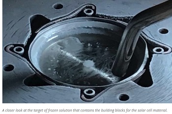
Adapted from a technology invented in 1999 called MAPLE, the technique involves freezing a solution containing the molecular building blocks for the perovskite, and then blasting the frozen block with a laser in a vacuum chamber.
When a laser vaporizes a small piece of the frozen target about the size of a dimple on a golf ball, the vapor travels upward in a plume that coats the bottom surface of any object hanging overhead, such as a component in a solar cell. Once enough of the material builds up, the process is stopped and the product is heated to crystallize the molecules and set the thin film in place.
In Stiff-Roberts’s version of the technology, the laser’s frequency is specifically tuned to the molecular bonds of the frozen solvent. This causes the solvent to absorb most of the energy, leaving the delicate organics unscathed as they travel to the product surface.
“The RIR-MAPLE technology is extremely gentle on the organic components of the material, much more so than other laser-based techniques,” said Stiff-Roberts. “That also makes it much more efficient, requiring only a small fraction of the organic materials to reach the same final product.”
Although no perovskite-based solar cells are yet available on the market, there are a few companies working to commercialize methylammonium lead iodide and other closely related materials. And while the materials made in this study have solar cell efficiencies better than those made with other laser-based technologies, they don’t yet reach those made with traditional solution-based processes.
But Mitzi and Stiff-Roberts say that’s not their goal.
“While solution-based techniques can also be gentle on organics and can make some great hybrid photovoltaic materials, they can’t be used for more complex and poorly soluble organic molecules,” said Stiff-Roberts.
“With this demonstration of the RIR-MAPLE technology, we hope to open a whole new world of materials to the solar cell industry,” continued Mitzi. “We also think these materials could be useful for other applications, such as light-emitting diodes, photodetectors and X-ray detectors.”
Share on:


Testimonial
"The I-Connect007 team is outstanding—kind, responsive, and a true marketing partner. Their design team created fresh, eye-catching ads, and their editorial support polished our content to let our brand shine. Thank you all! "
Sweeney Ng - CEE PCBSuggested Items
Meet the Author Podcast: Martyn Gaudion Unpacks the Secrets of High-Speed PCB Design
07/16/2025 | I-Connect007In this special Meet the Author episode of the On the Line with… podcast, Nolan Johnson sits down with Martyn Gaudion, signal integrity expert, managing director of Polar Instruments, and three-time author in I-Connect007’s popular The Printed Circuit Designer’s Guide to... series.
Intervala Hosts Employee Car and Motorcycle Show, Benefit Nonprofits
08/27/2024 | IntervalaIntervala hosted an employee car and motorcycle show, aptly named the Vala-Cruise and it was a roaring success! Employees had the chance to show off their prized wheels, and it was incredible to see the variety and passion on display.
KIC Honored with IPC Recognition for 25 Years of Membership and Contributions to Electronics Manufacturing Industry
06/24/2024 | KICKIC, a renowned pioneer in thermal process and temperature measurement solutions for electronics manufacturing, is proud to announce that it has been recognized by IPC for 25 years of membership and significant contributions to electronics manufacturing.
Boeing Starliner Spacecraft Completes Successful Crewed Docking with International Space Station
06/07/2024 | BoeingNASA astronauts Barry "Butch" Wilmore and Sunita "Suni" Williams successfully docked Boeing's Starliner spacecraft to the International Space Station (ISS), about 26 hours after launching from Cape Canaveral Space Force Station.
KIC’s Miles Moreau to Present Profiling Basics and Best Practices at SMTA Wisconsin Chapter PCBA Profile Workshop
01/25/2024 | KICKIC, a renowned pioneer in thermal process and temperature measurement solutions for electronics manufacturing, announces that Miles Moreau, General Manager, will be a featured speaker at the SMTA Wisconsin Chapter In-Person PCBA Profile Workshop.