


 Trouble in Your Tank: Implementing Direct Metallization in Advanced Substrate Packaging
 It’s Only Common Sense: Storytelling That Sells—Stop Pitching, Start Painting Pictures
 The Right Approach: Get Ready for ISO 9001 Version 6


NRL Improves Optical Efficiency in Nanophotonic Devices
January 5, 2018 | U.S. Naval Research LaboratoryEstimated reading time: 1 minute
A team of physicists, headed by the U.S. Naval Research Laboratory (NRL), have demonstrated the means to improve the optical loss characteristics and transmission efficiency of hexagonal boron nitride devices, enabling very small lasers and nanoscale optics.
“The applications for this research are considerably broad,” said Dr. Alexander J. Giles, research physicist, NRL Electronics Science and Technology Division. “By confining light to very small dimensions, nanophotonic devices have direct applications for use in ultra-high resolution microscopes, solar energy harvesting, optical computing and targeted medical therapies.”
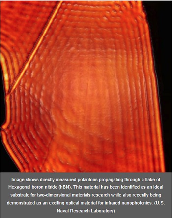
Hexagonal boron nitride (hBN) forms an atomically thin lattice consisting of boron and nitrogen atoms. This material has recently been demonstrated as an exciting optical material for infrared nanophotonics and is considered an ‘ideal substrate’ for two-dimensional materials.
While previous work demonstrated that natural hBN supports deeply sub-diffractional hyperbolic phonon polaritons desired for applications, such as, sub-diffractional optical imaging (so-called ‘hyperlensing’), energy conversion, chemical sensing, and quantum nanophotonics, limited transmission efficiencies continue to persist.
"We have demonstrated that the inherent efficiency limitations of nanophotonics can be overcome through the careful engineering of isotopes in polar semiconductors and dielectric materials,” Giles said.
Naturally occurring boron is comprised of two isotopes, boron-10 and boron-11, lending a 10 percent difference in atomic masses. This difference results in substantial losses due to phonon scattering, limiting the potential applications of this material. The research team at NRL has engineered greater than 99 percent isotopically pure samples of hBN, meaning they consist almost entirely of either boron-10 or boron-11 isotopes.
This approach results in a dramatic reduction in optical losses, resulting in optical modes that travel up to three times farther and persist for up to three times longer than natural hBN. These long-lived vibrational modes not only enable immediate advances specific to hBN — near field optics and chemical sensing — but also provide a strategic approach for other materials systems to exploit and build upon.
“Controlling and manipulating light at nanoscale, sub-diffractional dimensions is notoriously difficult and inefficient,” said Giles. “Our work represents a new path forward for the next generation of materials and devices.”
Contributors to this research include scientists from the University of California San Diego, Kansas State University, Oak Ridge National Laboratory, Columbia University, and Vanderbilt University. Full details of this research entitled “Ultralow-loss polaritons in isotopically pure boron nitride,” can be found in the December 11, 2017 edition of Nature Materials (doi:10.1038/nmat5047).
Share on:


Testimonial
"The I-Connect007 team is outstanding—kind, responsive, and a true marketing partner. Their design team created fresh, eye-catching ads, and their editorial support polished our content to let our brand shine. Thank you all! "
Sweeney Ng - CEE PCBSuggested Items
September 2025 PCB007 Magazine: The Future of Advanced Materials
09/16/2025 | I-Connect007 Editorial TeamMoore’s Law is no more, and the advanced material solutions being developed to grapple with this reality are surprising, stunning, and perhaps a bit daunting. Buckle up for a dive into advanced materials and a glimpse into the next chapters of electronics manufacturing.
I-Connect007 Launches Advanced Electronics Packaging Digest
09/15/2025 | I-Connect007I-Connect007 is pleased to announce the launch of Advanced Electronics Packaging Digest (AEPD), a new monthly digital newsletter dedicated to one of the most critical and rapidly evolving areas of electronics manufacturing: advanced packaging at the interconnect level.
Panasonic Industry will Double the Production Capacity of MEGTRON Multi-layer Circuit Board Materials Over the Next Five Years
09/15/2025 | Panasonic Industry Co., Ltd.Panasonic Industry Co., Ltd., a Panasonic Group company, announced plans for a major expansion of its global production capacity for MEGTRON multi-layer circuit board materials today. The company plans to double its production over the next five years to meet growing demand in the AI server and ICT infrastructure markets.
Trouble in Your Tank: Implementing Direct Metallization in Advanced Substrate Packaging
09/15/2025 | Michael Carano -- Column: Trouble in Your TankDirect metallization systems based on conductive graphite are gaining popularity throughout the world. The environmental and productivity gains achievable with this process are outstanding. Direct metallization reduces the costs of compliance, waste treatment, and legal issues related to chemical exposure. A graphite-based direct plate system has been devised to address these needs.
Fresh PCB Concepts: Designing for Success at the Rigid-flex Transition Area
08/28/2025 | Team NCAB -- Column: Fresh PCB ConceptsRigid-flex PCBs come in all shapes and sizes. Manufacturers typically use fire-retardant, grade 4 (FR-4) materials in the rigid section and flexible polyimide materials in the flex region. Because of the small size, some rigid-flex PCBs, like those for hearing aid devices, are among the most challenging to manufacture. However, regardless of its size, we should not neglect the transition area between the rigid and flexible material.