


 Trouble in Your Tank: Implementing Direct Metallization in Advanced Substrate Packaging
 It’s Only Common Sense: Storytelling That Sells—Stop Pitching, Start Painting Pictures
 The Right Approach: Get Ready for ISO 9001 Version 6


Lab Unlocks Secrets of Nanoscale 3D Printing
January 5, 2018 | Lawrence Livermore National LaboratoryEstimated reading time: 3 minutes
Lawrence Livermore National Laboratory (LLNL) researchers have discovered novel ways to extend the capabilities of two-photon lithography (TPL), a high-resolution 3D printing technique capable of producing nanoscale features smaller than one-hundredth the width of a human hair.
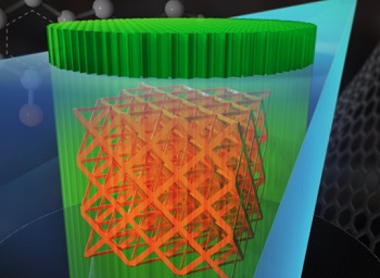
Image caption: LLNL researchers can print woodpile lattices with submicron features a fraction of the width of a human hair. Image by Jacob Long and Adam Connell/LLNL.
The findings, recently published on the cover of the journal ACS Applied Materials & Interfaces (link is external), also unleashes the potential for X-ray computed tomography (CT) to analyze stress or defects noninvasively in embedded 3D-printed medical devices or implants.
Two-photon lithography typically requires a thin glass slide, a lens and an immersion oil to help the laser light focus to a fine point where curing and printing occurs. It differs from other 3D-printing methods in resolution, because it can produce features smaller than the laser light spot, a scale no other printing process can match. The technique bypasses the usual diffraction limit of other methods because the photoresist material that cures and hardens to create structures — previously a trade secret — simultaneously absorbs two photons instead of one.
LLNL researchers printed octet truss structures with submicron features on top of a solid base with a diameter similar to human hair. Photo by James Oakdale/LLNL.
In the paper, LLNL researchers describe cracking the code on resist materials optimized for two-photon lithography and forming 3D microstructures with features less than 150 nanometers. Previous techniques built structures from the ground up, limiting the height of objects because the distance between the glass slide and lens is usually 200 microns or less. By turning the process on its head — putting the resist material directly on the lens and focusing the laser through the resist — researchers can now print objects multiple millimeters in height. Furthermore, researchers were able to tune and increase the amount of X-rays the photopolymer resists could absorb, improving attenuation by more than 10 times over the photoresists commonly used for the technique.
“In this paper, we have unlocked the secrets to making custom materials on two-photon lithography systems without losing resolution,” said LLNL researcher James Oakdale, a co-author on the paper.
Because the laser light refracts as it passes through the photoresist material, the linchpin to solving the puzzle, the researchers said, was “index matching” – discovering how to match the refractive index of the resist material to the immersion medium of the lens so the laser could pass through unimpeded. Index matching opens the possibility of printing larger parts, they said, with features as small as 100 nanometers.
“Most researchers who want to use two-photon lithography for printing functional 3D structures want parts taller than 100 microns,” said Sourabh Saha, the paper’s lead author. “With these index-matched resists, you can print structures as tall as you want. The only limitation is the speed. It’s a tradeoff, but now that we know how to do this, we can diagnose and improve the process.”
Through the two-photon lithography (TPL) 3D printing process, researchers can print woodpile lattices with submicron features a fraction of the width of a human hair. Photo by James Oakdale/LLNL.
By tuning the material’s X-ray absorption, researchers can now use X-ray-computed tomography as a diagnostic tool to image the inside of parts without cutting them open or to investigate 3D-printed objects embedded inside the body, such as stents, joint replacements or bone scaffolds. These techniques also could be used to produce and probe the internal structure of targets for the National Ignition Facility, as well as optical and mechanical metamaterials and 3D-printed electrochemical batteries.
The only limiting factor is the time it takes to build, so researchers will next look to parallelize and speed up the process. They intend to move into even smaller features and add more functionality in the future, using the technique to build real, mission-critical parts.
“It’s a very small piece of the puzzle that we solved, but we are much more confident in our abilities to start playing in this field now,” Saha said. “We’re on a path where we know we have a potential solution for different types of applications. Our push for smaller and smaller features in larger and larger structures is bringing us closer to the forefront of scientific research that the rest of the world is doing. And on the application side, we’re developing new practical ways of printing things.”
The work was funded through the Laboratory Directed Research and Development (LDRD) program. Other LLNL researchers who contributed to the project include Jefferson Cuadra, Chuck Divin, Jianchao Ye, Jean-Baptiste Forien, Leonardus Bayu Aji, Juergen Biener and Will Smith.
Share on:


Testimonial
"We’re proud to call I-Connect007 a trusted partner. Their innovative approach and industry insight made our podcast collaboration a success by connecting us with the right audience and delivering real results."
Julia McCaffrey - NCAB GroupSuggested Items
Advint Incorporated Brings Artificial Intelligence to Electroplating Training
09/11/2025 | Advint IncorporatedAdvint Incorporated is introducing a new dimension to its electroplating training programs: the integration of Artificial Intelligence (AI). This initiative reflects the company’s commitment to providing PCB fabricators and manufacturers in the USA and Canada with training that is practical, forward-looking, and directly relevant to today’s production challenges.
The Signal Integrity Issue: Design007 Magazine September 2025
09/09/2025 | I-Connect007 Editorial TeamAs the saying goes, “If you don’t have signal integrity problems now, you will eventually.” This month, our experts share a variety of design techniques that can help PCB designers and design engineers achieve signal integrity.
Semiconductors Get Magnetic Boost with New Method from UCLA Researchers
07/31/2025 | UCLA NewsroomA new method for combining magnetic elements with semiconductors — which are vital materials for computers and other electronic devices — was unveiled by a research team led by the California NanoSystems Institute at UCLA.
SMT Perspectives and Prospects: Warren Buffett’s Perpetual Wisdom, Part 1
07/29/2025 | Dr. Jennie Hwang -- Column: SMT Perspectives and ProspectsOver the years, I have cherished the lessons by Warren Buffett and Charlie Munger at the Berkshire Hathaway annual shareholders meeting in Omaha, Nebraska. This year, I was among the more than 40,000 who attended the May 3 meeting. Millions more from around the world, including from the UK, Germany, Japan, China, Panama, and Guatemala, tuned in remotely and via CNBC’s livestream.
Mesa West, Advanced West Announce Strategic Partnership
06/15/2025 | I-Connect007Mesa West is proud to announce that they have officially joined forces with Advanced West. This strategic partnership brings together two industry leaders, uniting strengths to better serve customers through enhanced capabilities, expanded offerings, and continued commitment to quality.