


 Trouble in Your Tank: Implementing Direct Metallization in Advanced Substrate Packaging
 It’s Only Common Sense: Storytelling That Sells—Stop Pitching, Start Painting Pictures
 The Right Approach: Get Ready for ISO 9001 Version 6


What’s the Noise Eating Quantum Bits?
January 10, 2018 | Department of Energy, Office of ScienceEstimated reading time: 2 minutes
Super powerful quantum computing relies on quantum bits, aka qubits, which are the equivalent of the classical bits used in today’s computers. SQUIDs are being investigated for the development of qubits. However, system noise can destroy the data stored in the resulting qubits.
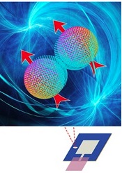
Image caption: Noise is an obstacle in the race to realize systems that can be used to develop quantum computing technologies. Among the approaches for quantum computing is the superconducting quantum interference device (SQUID), shown at the bottom of the figure. Researchers have shown that the main source of noise is magnetic defects on the SQUID. These defects are produced by molecular oxygen (O2) adsorbed on its surface. The artistic drawing is of magnetic noise from molecular oxygen. The sketch shows twisted magnetic field lines induced by harmful fluctuating magnetic spins (arrows) of O2 (spheres) on the surface of a SQUID quantum bit. Image courtesy of junyiwu.com
Calculations have confirmed experimental evidence that oxygen molecules adsorbed on the surface of the SQUID are the most likely source of low-frequency magnetic noise. Scientists identified mitigation strategies, such as surface protection and improved vacuum environments. These approaches lowered the surface oxygen and the associated noise to levels needed for SQUIDs to be used in the next generation of computers.
Superconducting devices are candidates for developing qubits. One type of device is called a SQUID for superconducting quantum interference device. It is based on a superconducting loop containing one or two Josephson junctions and allows measurement of quantized magnetic energy. However, the ability to develop SQUID-based quantum computers will require the stored magnetic data survive for long times. Scientists discovered the origin of magnetic noise in these systems, and ways to minimize it. Their work provides a design strategy for the development of tunable superconducting qubits with long lifetimes.
In quantum computing, quantum information is lost due to a loss of synchronization (dephasing) in the electronic flow and energy relaxation. Magnetic flux noise is a dominant source of dephasing and energy relaxation in superconducting qubits. Recently reported experiments indicated that the detrimental noise is from unpaired magnetic defects on surfaces of superconducting devices.
Theoretical predictions singled out oxygen as the cause of noise in these systems. In a team effort, theory calculations at the University of California, Irvine and experimental measurements by their collaborators showed that adsorbed molecular oxygen (O2 on the surfaces is the dominant contributor to magnetic noise for superconducting niobium and aluminum thin films. The mechanism is related to the outermost electrons of the oxygen molecule forming a magnetic spin-1 triplet state. Theory and experiment were iterated to find mitigation strategies. Surface treatment with ammonia and improving the sample vacuum environment dramatically reduced the surface contamination (to less than one oxygen molecule per 10 nm2), minimizing magnetic noise. In x-ray experiments at the Advanced Photon Source, scientists measured the suppression of magnetic spin and magnetic noise. Molecular oxygen was confirmed as the extrinsic noise source. The identification of this source explains the weak dependence of this type of noise on device materials. Also, discovering the origin of this noise invalidates prevailing theories for the noise based on defects at the metal-insulator interface. Suitable surface protection and improvements in the vacuum can lead to significant reductions in low-frequency magnetic noise. This new understanding of the origin of magnetic flux noise could lead to frequency-tunable superconducting qubits with improved dephasing times for practical quantum computers.
Share on:


Testimonial
"Our marketing partnership with I-Connect007 is already delivering. Just a day after our press release went live, we received a direct inquiry about our updated products!"
Rachael Temple - AlltematedSuggested Items
Driving Innovation: Depth Routing Processes—Achieving Unparalleled Precision in Complex PCBs
09/08/2025 | Kurt Palmer -- Column: Driving InnovationIn PCB manufacturing, the demand for increasingly complex and miniaturized designs continually pushes the boundaries of traditional fabrication methods, including depth routing. Success in these applications demands not only on robust machinery but also sophisticated control functions. PCB manufacturers rely on advanced machine features and process methodologies to meet their precise depth routing goals. Here, I’ll explore some crucial functions that empower manufacturers to master complex depth routing challenges.
Polar Instruments Announces Additive Transmission Line Support for Si9000e
08/20/2025 | Polar InstrumentsTransmission lines embedded into the PCB surface are a feature of UHDI constructions. The 2025 fall release of Polar's Si9000e PCB impedance & insertion loss transmission line field solver incorporates eight new single ended, differential and coplanar transmission line structures.
Henniker Plasma Launches Stratus Turnkey Plasma Manufacturing Cell
08/13/2025 | Henniker PlasmaHenniker Plasma, a leading manufacturer of plasma treatment systems, proudly announces the launch of its Stratus Plasma Manufacturing Cell range — a fully integrated, turnkey solution that combines advanced atmospheric plasma surface treatment with robotic automation.
Trouble in Your Tank: Metallizing Flexible Circuit Materials—Mitigating Deposit Stress
08/04/2025 | Michael Carano -- Column: Trouble in Your TankMetallizing materials, such as polyimide used for flexible circuitry and high-reliability multilayer printed wiring boards, provide a significant challenge for process engineers. Conventional electroless copper systems often require pre-treatments with hazardous chemicals or have a small process window to achieve uniform coverage without blistering. It all boils down to enhancing the adhesion of the thin film of electroless copper to these smooth surfaces.
Designers Notebook: Basic PCB Planning Criteria—Establishing Design Constraints
07/22/2025 | Vern Solberg -- Column: Designer's NotebookPrinted circuit board development flows more smoothly when all critical issues are predefined and understood from the start. As a basic planning strategy, the designer must first consider the product performance criteria, then determine the specific industry standards or specifications that the product must meet. Planning also includes a review of all significant issues that may affect the product’s manufacture, performance, reliability, overall quality, and safety.