


 Trouble in Your Tank: Implementing Direct Metallization in Advanced Substrate Packaging
 It’s Only Common Sense: Storytelling That Sells—Stop Pitching, Start Painting Pictures
 The Right Approach: Get Ready for ISO 9001 Version 6


Bendable Touch Panel Achieved with Silver Nano Ink Printing Technology
January 17, 2018 | ACN NewswireEstimated reading time: 4 minutes
JST has recognized the results of NexTEP's project, "A Sensor Film for Touch Panels Using Thin Metallic Wire" as a success.
This development task was based on the research of Professor Tatsuo Hasegawa, Principal Research Manager at the Flexible Electronics Research Center of the National Institute of Advanced Industrial Science and Technology, and was consigned to Tanaka Kikinzoku Kogyo (Representative Director & CEO, Akira Tanae, Chiyoda-ku, Tokyo) from April 2014 through September 2017. The research proceeded with the aim of practical application through Tanaka Kikinzoku Kogyo's Global Marketing/R&D Division.
In conventional electrostatic capacity-type touch panels, indium tin oxide (ITO) is used for the sensor. However, because of its high electrical resistivity and weakness upon bending, companies faced difficulties in increasing the size of such sensors and making them more flexible. Metal mesh (MM) solves these problems, but it is difficult to make thinner than 4 um, and no technology existed to manufacture the mesh via printing.
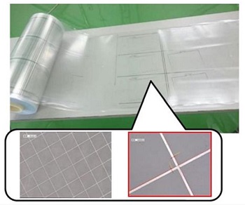
To apply the new technology (SuPR-NaP method), which fabricates wiring through an adsorption reaction between special silver ink and an activated fluororesin surface, at a suitable speed for commercial manufacturing, the project clarified the reaction mechanism and researched the development of manufacturing equipment as well as the conditions for each process. As a result, the project constructed a system for manufacturing MM film (line width: 2-4 um) with the full process roll-to-roll method*5. In a 200,000-frequency (radius: 2 mm) bending test, this MM film exhibits hardly any changes in resistance values, and it has cleared general reliability testing.
This success in manufacturing the world's first micro-wiring film with a full process roll-to-roll method is an important technological innovation in printed electronics for the flexible electronic device market. It is also anticipated that the technology could be applied and used for applications requiring metal patterns on resin film (function films e.g. antibacterial, catalyst, thermal insulating).
With the increased use of information technology in society, people are demanding access to information in various locations, at various times and in various situations. Touch panels that are integrated with the display are used in many devices, from smartphones, notebooks, large panel to automotive displays.
Moreover, touch sensors now need to be compatible with not only flat panel displays, but also recently-announced three-dimensional curved and bendable displays. Transparent (conducting) electrodes using ITO are mainly used for current touch sensors. However, physical problems such as high electrical resistivity and weakness upon bending imposed limitations on responding to needs for flexibility and increasingly large screen sizes. Metal mesh(MM), in which thin metallic wire is used as the electrode, is being applied on as a material that could solve these problems. However, as the line width and pitch of current MM is thick, the wiring is visible on smartphones, which are used at a short distance. Therefore, it has only come into popular use for large displays.
Development Details
With this new printing technology, a film to which liquid-repelling fluororesin is applied undergoes pattern exposure through a photo mask. Metal ink is then scanned onto it to form the wiring. This technology means that metal wiring with a fixed film thickness can be formed by means of the chemisorption of metal nanoparticles on the fluororesin surface activated by light.
The following technology has been developed to make it possible to manufacture MM film with micro wiring that can also be used for smartphones at a low cost. The project constructed a roll-to-roll production system that has not been available with existing manufacturing methods.
- The reaction mechanism for printing was elucidated, ink and fluororesin which was investigated and a method of even printing on large areas was developed. This made it possible to fabricate a 7- to 8-inch sensor film with micro wiring (line width: 2-4 um).
- Invisible wiring was developed by postprocessing the sensor pattern design (line width and shape) to respond to market needs. As a result, a MM film that could also be used for smartphones was able to be developed. The ability of this film to withstand 200,000-frequency (radius: 2 mm) bending test was also confirmed.
- Equipment for each process was developed and a manufacturing method with the roll-to-roll process was established. In a manufacturing experiment for the line width 4 um MM film, the 10m roll length achieved more than a 95% yield rate was achieved.
Anticipated Effects
This successful development is expected to enable the low-cost manufacturing of high-functioning touch panel sensor films that can be used for three-dimensional curved or bendable displays.
This manufacturing of a micro wiring film with full process roll-to-roll process is the first of its kind in the world. It is a breakthrough technological innovation for printed electronics used in the flexible electronic device market. It is anticipated that this technology can be not only applied and used in electronics fields such as OLED*6 displays, IoT device wiring and electrodes, but also in the manufacturing of functional films such as antibacterial films, films for catalysts and thermal insulation films.
Share on:


Testimonial
"Our marketing partnership with I-Connect007 is already delivering. Just a day after our press release went live, we received a direct inquiry about our updated products!"
Rachael Temple - AlltematedSuggested Items
Siemens, TRUMPF Partner to Accelerate Digital Manufacturing and AI Readiness
09/16/2025 | SiemensTechnology company Siemens and leading machine tools and laser manufacturer TRUMPF announced a partnership that promises to elevate industrial production by harnessing advanced digital manufacturing solutions.
I-Connect007 Launches Advanced Electronics Packaging Digest
09/15/2025 | I-Connect007I-Connect007 is pleased to announce the launch of Advanced Electronics Packaging Digest (AEPD), a new monthly digital newsletter dedicated to one of the most critical and rapidly evolving areas of electronics manufacturing: advanced packaging at the interconnect level.
ICAPE Group Unveils Exclusive Report on Sustainability in Electronics Manufacturing
09/15/2025 | ICAPE GroupICAPE Group, a global leader in printed circuit boards (PCBs) and custom electronics manufacturing, today announces the launch of its 2025 Industry Outlook & Innovation Report: Sustainability in Electronics Manufacturing. This exclusive report is accompanied by fresh insights from a dedicated Statista survey of 100 electronics manufacturing professionals, commissioned by ICAPE Group.
Panasonic Industry will Double the Production Capacity of MEGTRON Multi-layer Circuit Board Materials Over the Next Five Years
09/15/2025 | Panasonic Industry Co., Ltd.Panasonic Industry Co., Ltd., a Panasonic Group company, announced plans for a major expansion of its global production capacity for MEGTRON multi-layer circuit board materials today. The company plans to double its production over the next five years to meet growing demand in the AI server and ICT infrastructure markets.
Sustainability and Selective Soldering
09/15/2025 | Dr. Samuel J. McMaster, Pillarhouse InternationalSustainability is more than just a buzzword for the electronics industry; it’s a key goal for all manufacturing processes. This is more than a box-ticking exercise or simply doing a small part for environmentally friendly processes. Moving toward sustainable solutions drives innovation and operational efficiency.