


 Trouble in Your Tank: Implementing Direct Metallization in Advanced Substrate Packaging
 It’s Only Common Sense: Storytelling That Sells—Stop Pitching, Start Painting Pictures
 The Right Approach: Get Ready for ISO 9001 Version 6


Building Blocks to Create Metamaterials
January 18, 2018 | CaltechEstimated reading time: 4 minutes
Engineers at Caltech and ETH Zürich in Switzerland have created a method to systematically design metamaterials using principles of quantum mechanics.
Their work could pave the way for wider use of metamaterials in more mainstream applications by creating a purpose-driven framework for their design.
Metamaterials are engineered materials that exploit the geometry of their internal structure to manipulate incoming waves. For example, a metamaterial that manipulates electromagnetic waves might bend light in an unusual way to create a cloaking device. Meanwhile, a wafer-thin acoustic metamaterial might reflect incoming sound waves to soundproof a room.
This ability to control waves derives from how the material is structured, often on a microscopic scale. In 2010, Caltech researchers developed an optical metamaterial that uses a surface coated with three-dimensional structures to redirect light as desired. More recently, engineers at Caltech showed that flat surfaces coated with tiny pillars of silicon could focus light like a lens.
Picture a crystal—a solid whose physical properties are determined by the way it is built from a repeating series of atomic structures. Carbon atoms structured in flat plates create crumbly graphite, while carbon atoms structured in tetrahedra create ultra-hard diamonds. Similarly, metamaterials are constructed from a repeating series of nano- and micro-scale structures that give them their unique properties.
Despite their promise and wide array of possible applications, metamaterials will not be used widely unless engineers can design them to have particular desired properties. While much progress has been made in the design of metamaterials that interact with electromagnetic waves, overall, the design of mechanical metamaterials—those that influence mechanical waves, such as sound waves or seismic waves—remains a scattershot affair, says Chiara Daraio, a professor of mechanical engineering and applied physics at Caltech.
"Before our work, there was no single, systematic way to design metamaterials that control mechanical waves for different applications," she says. "Instead, people often optimized a design to fulfill a specific purpose, or tried out new designs based on something they saw in nature, and then studied what properties would arise from repeated patterns."
To address this, a team led by Daraio and consisting of graduate students Marc Serra Garcia and Antonio Palermo, postdoctoral scholar Katie Matlack, and professor Sebastian Huber at ETH Zürich, turned to the field of quantum mechanics. On the surface, the choice was an unlikely one. Quantum mechanics governs the often-counterintuitive behavior of subatomic particles, and would seem to have no bearing on the micro- and macro-scale designs of the metamaterials studied by Daraio's team.
Quantum mechanics predicts the existence of certain exotic types of matter: among them, a "topological insulator" that conducts electricity across its surface while acting as an insulator in its interior. Daraio's team realized that they could build macro-scale versions of these exotic systems that could conduct and insulate against vibrations instead of electricity by using principles of quantum mechanics. In quantum mechanics, materials can sometimes be described as an ensemble of interacting particles. "Imagine that each particle is a tiny mass, connected to its neighbors by springs," she explains. "Each particle reacts to incoming waves in a unique way that is determined, in part, by the reaction of its neighbors. In our approach, we apply this mass-and-spring model to macroscopic, elastic materials, maintaining their characteristic properties."
Because metamaterials are built from arrays of geometrical structures (that can have building blocks at the nano-, micro-, or macro-scale) that are connected in repeating patterns, Daraio and her colleagues realized that, by representing each repeating structure as an ensemble of particles, it would be possible to design many different types of metamaterials, like waveguides, acoustic lenses, or vibration insulators.
When struck by an incoming wave, each repeating structure in a metamaterial has the potential to deform in a number of different ways. That deformation is governed not only by the geometry of that structure, but also by how the structures are connected and how the other structures around them are reacting. Treating this as a system of masses and springs, Daraio's team was able to predict how these systems would react, and then engineer them to react in desired ways.
It is complicated, but also predictable—which is the important part.
As a theoretical proof of concept, Daraio's team designed metamaterials made from a series of rectangular millimeter-scale plates, each loosely connected to one another like a piece of a puzzle. By tuning the design of the plates and how well-connected the plates were, the team created a perfect acoustic lens that focuses sound without loss of signal. The plates also act as a waveguide that directs and slows the propagation of sound. The method could be used to design many other devices or sensors where high sensitivity, precision, or control are necessary, Daraio says. The work was published in Nature Materials on January 15.
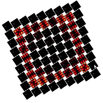
Though Daraio's work is theoretical, validated using computer simulations, her coauthors at ETH used the method to design and build a 10 by 10-centimeter silicon wafer that consists of 100 small plates connected to each other via thin beams. When the wafer is stimulated using ultrasound, only the plates in the corners vibrate; the other plates remain still, despite their connections. The device could be used as a precise waveguide in a communications network. Their work was published in Nature on January 15.
The design process described can also be used to design optical metamaterials, antennas, and optical signal processing devices, says Daraio. Their paper is titled "Designing perturbative metamaterials from discrete models." This work was funded by ETH Zürich and the Swiss National Science Foundation.
Share on:


Testimonial
"We’re proud to call I-Connect007 a trusted partner. Their innovative approach and industry insight made our podcast collaboration a success by connecting us with the right audience and delivering real results."
Julia McCaffrey - NCAB GroupSuggested Items
ASM Technologies Limited signs MoU with the Guidance, Government of Tamilnadu to Expand Design-Led Manufacturing capabilities for ESDM
09/15/2025 | ASM TechnologiesASM Technologies Limited, a pioneer in Design- Led Manufacturing in the semiconductor and automotive industries, announced signing of Memorandum of Understanding (MoU) with the Guidance, Government of Tamilnadu whereby it will invest Rs. 250 crores in the state to expand its ESDM related Design-Led Manufacturing and precision engineering capacity. ASM Technologies will acquire 5 acres of land from the Government of Tamilnadu to set up a state-of-the-art design facility in Tamil Nadu's growing technology manufacturing ecosystem, providing a strong strategic advantage and long-term benefits for ASM.
Variosystems Strengthens North American Presence with Southlake Relaunch 2025
09/15/2025 | VariosystemsVariosystems celebrated the relaunch of its U.S. facility in Southlake, Texas. After months of redesign and reorganization, the opening marked more than just the return to a modernized production site—it was a moment to reconnect with our teams, partners, and the local community.
Deca, Silicon Storage Technology Announce Strategic Collaboration to Enable NVM Chiplet Solutions
09/11/2025 | Microchip Technology Inc.As traditional monolithic chip designs grow in complexity and increase in cost, the interest and adoption of chiplet technology in the semiconductor industry also increases.
I-Connect007 Launches New Podcast Series on Ultra High Density Interconnect (UHDI)
09/10/2025 | I-Connect007I-Connect007 is excited to announce the debut of its latest podcast series, which shines a spotlight on one of the most important emerging innovations in electronics manufacturing: Ultra-High-Density Interconnect (UHDI). The series kicks off with Episode One, “Ultra HDI: What does it mean to people? Why would they want it?” Host Nolan Johnson is joined by guest expert John Johnson, Director of Quality and Advanced Technology at American Standard Circuits (ASC).
Global Citizenship: Together for a Perfect PCB Solution
09/10/2025 | Tom Yang -- Column: Global CitizenshipIf there’s one thing we’ve learned in the past few decades of electronics evolution, it’s that no region has a monopoly on excellence. Whether it’s materials science breakthroughs in Europe, manufacturing efficiencies in China, or design innovations in Silicon Valley, the PCB industry thrives on collaboration.