


 Trouble in Your Tank: Implementing Direct Metallization in Advanced Substrate Packaging
 It’s Only Common Sense: Storytelling That Sells—Stop Pitching, Start Painting Pictures
 The Right Approach: Get Ready for ISO 9001 Version 6


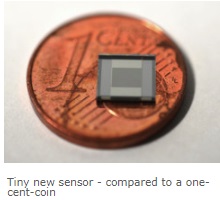
New Sensor for Measuring Electric Field Strength
January 25, 2018 | Technische Universität WienEstimated reading time: 2 minutes
Accurately measuring electric fields is important in a variety of applications, such as weather forecasting, process control on industrial machinery, or ensuring the safety of people working on high-voltage power lines. Yet from a technological perspective, this is no easy task.
In a break from the design principle that has been followed by all other measuring devices to date, a research team at TU Wien has now developed a silicon-based sensor as a microelectromechanical system (MEMS). Devised in conjunction with the Department for Integrated Sensor Systems at Danube University Krems, this sensor has the major advantage that it does not distort the very electric field it is currently measuring. An introduction to the new sensor has also been published in the electronics journal "Nature Electronics".
Distorting measuring devices
"The equipment currently used to measure electric field strength has some significant downsides," explains Andreas Kainz from the Institute of Sensor and Actuator Systems (Faculty of Electrical Engineering, TU Wien). "These devices contain parts that become electrically charged. Conductive metallic components can significantly alter the field being measured; an effect that becomes even more pronounced if the device also has to be grounded to provide a reference point for the measurement." Such equipment also tends to be relatively impractical and difficult to transport.
The sensor developed by the team at TU Wien is made from silicon and is based on a very simple concept: small, grid-shaped silicon structures measuring just a few micrometres in size are fixed onto a small spring. When the silicon is exposed to an electric field, a force is exerted on the silicon crystals, causing the spring to slightly compress or extend.
These tiny movements now need to be made visible, for which an optical solution has been designed: an additional grid located above the movable silicon grid is lined up so precisely that the grid openings on one grid are concealed by the other. When an electric field is present, the movable structure moves slightly out of perfect alignment with the fixed grid, allowing light to pass through the openings. This light is measured, from which the strength of the electric field can be calculated by an appropriately calibrated device.
Prototype achieves impressive levels of precision
The new silicon sensor does not measure the direction of the electric field, but its strength. It can be used for fields of a relatively low frequency of up to one kilohertz. "Using our prototype, we have been able to reliably measure weak fields of less than 200 volts per metre," says Andreas Kainz. "This means our system is already performing at roughly the same level as existing products, even though it is significantly smaller and much simpler." And there is still a great deal of potential for improvement, too: "Other methods of measurement are already mature approaches – we are just starting out. In future it will certainly be possible to achieve even significantly better results with our microelectromechanical sensor," adds Andreas Kainz confidently.
Share on:


Testimonial
"Advertising in PCB007 Magazine has been a great way to showcase our bare board testers to the right audience. The I-Connect007 team makes the process smooth and professional. We’re proud to be featured in such a trusted publication."
Klaus Koziol - atgSuggested Items
Electra’s ElectraJet EMJ110 Inkjet Soldermask Now in Black & Blue at Sunrise Electronics
09/08/2025 | Electra Polymers LtdFollowing the successful deployment of Electra’s Green EMJ110 Inkjet Soldermask on KLA’s Orbotech Neos™ platform at Sunrise Electronics in Elk Grove Village, Illinois, production has now moved beyond green.
Magnachip Semiconductor Announces YJ Kim to Step Down as CEO; Current Board Chairman Camillo Martino Appointed Interim CEO
08/14/2025 | PR NewswireMagnachip Semiconductor Corporation today announced that YJ Kim has agreed to step down as CEO and as a member of the Board of Directors, effective immediately. Camillo Martino, Chairman of the Board of Directors, has also been appointed Interim Chief Executive Officer, effective immediately.
Bell to Build X-Plane for Phase 2 of DARPA Speed and Runway Independent Technologies (SPRINT) X-Plane Program
07/09/2025 | Bell Textron Inc.Bell Textron Inc., a Textron Inc. company, has been down-selected for Phase 2 of Defense Advanced Research Projects Agency (DARPA) Speed and Runway Independent Technologies (SPRINT) X-Plane program with the objective to complete design, construction, ground testing and certification of an X-plane demonstrator.
Nolan’s Notes: Moving Forward With Confidence
06/03/2025 | Nolan Johnson -- Column: Nolan's NotesWe’re currently enjoying a revitalized and dynamic EMS provider market with significant growth potential. Since December 2024, the book-to-bill has been extremely strong and growing. Starting with a ratio of 1.24 in December, book-to-bill has continued to accelerate to a 1.41 in April. Yet, there is a global economic restructuring taking place. To say that the back-and-forth with tariffs and trade deals makes for an uncertain market is an understatement. While we may be in a 90-day tariff pause among leading economic nations, the deadline is quickly approaching and that leaves many of you feeling unsettled about what to expect.
Mycronic High Flex Changes Division Name to PCB Assembly Solutions
05/20/2025 | MycronicMycronic AB, the leading Sweden-based electronics assembly solutions provider, announced that its division formerly known as High Flex will now operate under the name PCB Assembly Solutions.