


 Trouble in Your Tank: Implementing Direct Metallization in Advanced Substrate Packaging
 It’s Only Common Sense: Storytelling That Sells—Stop Pitching, Start Painting Pictures
 The Right Approach: Get Ready for ISO 9001 Version 6


Flexible, Water-Repellent Graphene Circuits for Washable Electronics
January 25, 2018 | Iowa State UniversityEstimated reading time: 2 minutes
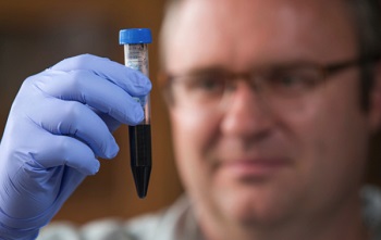
New graphene printing technology can produce electronic circuits that are low-cost, flexible, highly conductive and water repellent.
The nanotechnology “would lend enormous value to self-cleaning wearable/washable electronics that are resistant to stains, or ice and biofilm formation,” according to a recent paper describing the discovery.
“We’re taking low-cost, inkjet-printed graphene and tuning it with a laser to make functional materials,” said Jonathan Claussen, an Iowa State University assistant professor of mechanical engineering, an associate of the U.S. Department of Energy’s Ames Laboratory and the corresponding author of the paper recently featured on the cover of the journal Nanoscale.
The paper describes how Claussen and the nanoengineers in his research group use inkjet printing technology to create electric circuits on flexible materials. In this case, the ink is flakes of graphene – the wonder material can be a great conductor of electricity and heat, plus it’s strong, stable and biocompatible.
The printed flakes, however, aren’t highly conductive and have to be processed to remove non-conductive binders and weld the flakes together, boosting conductivity and making them useful for electronics or sensors.
That post-print process typically involves heat or chemicals. But Claussen and his research group developed a rapid-pulse laser process that treats the graphene without damaging the printing surface – even if it’s paper.
And now they’ve found another application of their laser processing technology: taking graphene-printed circuits that can hold water droplets (they’re hydrophilic) and turning them into circuits that repel water (they’re superhydrophobic).
“We’re micro-patterning the surface of the inkjet-printed graphene,” Claussen said. “The laser aligns the graphene flakes vertically – like little pyramids stacking up. And that’s what induces the hydrophobicity.”
Claussen said the energy density of the laser processing can be adjusted to tune the degree of hydrophobicity and conductivity of the printed graphene circuits.
And that opens up all kinds of possibilities for new electronics and sensors, according to the paper.
“One of the things we’d be interested in developing is anti-biofouling materials,” said Loreen Stromberg, a paper co-author and an Iowa State postdoctoral research associate in mechanical engineering and for the Virtual Reality Applications Center. “This could eliminate the buildup of biological materials on the surface that would inhibit the optimal performance of devices such as chemical or biological sensors.”
The technology could also have applications in flexible electronics, washable sensors in textiles, microfluidic technologies, drag reduction, de-icing, electrochemical sensors and technology that uses graphene structures and electrical simulation to produce stem cells for nerve regeneration.
The researchers wrote that further studies should be done to better understand how the nano- and microsurfaces of the printed graphene creates the water-repelling capabilities.
The current studies have been supported by grants from the National Science Foundation, the U.S. Department of Agriculture’s National Institute of Food and Agriculture, the Roy J. Carver Charitable Trust plus Iowa State’s College of Engineering and department of mechanical engineering.
The Iowa State University Research Foundation is working to patent the technology and has optioned it to an Ames-based startup, NanoSpy Inc., for possible commercialization. NanoSpy, located at the Iowa State University Research Park, is developing sensors to detect salmonella and other pathogens in food processing plants. Claussen and Stromberg are part of the company.
The graphene printing, processing and tuning technology is turning out to be very useful, Stromberg said. After all, “electronics are being incorporated into everything.”
Share on:


Testimonial
"Advertising in PCB007 Magazine has been a great way to showcase our bare board testers to the right audience. The I-Connect007 team makes the process smooth and professional. We’re proud to be featured in such a trusted publication."
Klaus Koziol - atgSuggested Items
Beyond the Board: What Companies Need to Know Before Entering the MilAero PCB Market
09/16/2025 | Jesse Vaughan -- Column: Beyond the BoardThe MilAero electronics supply chain offers opportunities for manufacturers that are both prestigious and strategically important. Serving prime contractors and Tier-1 suppliers can mean long-term program stability and the satisfaction of contributing to national security. At the same time, this sector is unlike commercial electronics in almost every respect. Success requires more than technical capabilities, it requires patience, preparation, attention to detail, and a clear understanding of how the business model differs.
India’s Aerospace and Defence Engineered for Power, Driven by Electronics
09/16/2025 | Gaurab Majumdar, Global Electronics AssociationWith a defence budget of $82.05 billion (2025–26) and a massive $223 billion earmarked for aerospace and defence spending over the next decade, India is rapidly positioning itself as a major player in the global defence and aerospace market.
I-Connect007 Launches Advanced Electronics Packaging Digest
09/15/2025 | I-Connect007I-Connect007 is pleased to announce the launch of Advanced Electronics Packaging Digest (AEPD), a new monthly digital newsletter dedicated to one of the most critical and rapidly evolving areas of electronics manufacturing: advanced packaging at the interconnect level.
Global Interposer Market to Surge Nearly Fivefold by 2034
09/15/2025 | I-Connect007 Editorial TeamRevenue for the global interposer market is projected to climb from $471 million in 2025 to more than $2.3 billion by 2034, according to a new report from Business Research Insights. The growth represents a CAGR of nearly 20 percent over the forecast period.
ICAPE Group Unveils Exclusive Report on Sustainability in Electronics Manufacturing
09/15/2025 | ICAPE GroupICAPE Group, a global leader in printed circuit boards (PCBs) and custom electronics manufacturing, today announces the launch of its 2025 Industry Outlook & Innovation Report: Sustainability in Electronics Manufacturing. This exclusive report is accompanied by fresh insights from a dedicated Statista survey of 100 electronics manufacturing professionals, commissioned by ICAPE Group.