


 Trouble in Your Tank: Implementing Direct Metallization in Advanced Substrate Packaging
 It’s Only Common Sense: Storytelling That Sells—Stop Pitching, Start Painting Pictures
 The Right Approach: Get Ready for ISO 9001 Version 6


A Simpler Path
January 29, 2018 | A*STAREstimated reading time: 2 minutes
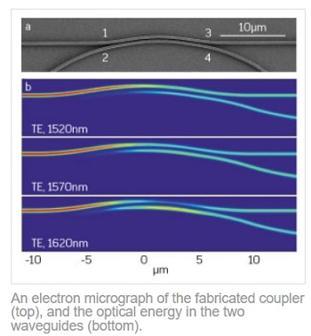
A core element of circuits handling optical signals can now be made smaller and simpler, and with functionality over a wider range of wavelengths, because of a mathematical model developed by A*STAR researchers. The new design methodology is expected to have widespread use in photonic integrated circuits and contribute to more compact photonic devices.
Optical signals, such as those transmitted over optical fiber, require photonic elements and circuits to be useful. One of the most important photonic functions is ‘coupling’, which allows the signal to be split into two different paths or used to drive other dependent circuits. Coupling, however, is generally only reliable over a narrow band of wavelengths, demanding a complicated design and fabrication process and bulkier circuits.
To overcome this obstacle to photonic circuit miniaturization, Jun Rong Ong and colleagues from the A*STAR Institute of High Performance Computing, in collaboration with researchers from the Singapore University of Technology and Design, went back to the drawing board to find a simpler approach to designing these critical coupling elements for broadband operation.
“Couplers are the basic building blocks of photonic circuits,” explains Ong. “However, it has been very difficult to try to make them compact, with low power loss and broadband operability, using standard processes.”
A coupler works by running a second optical path, known as a waveguide, alongside the signal path. The optical signal induces a secondary signal in the adjacent waveguide, passing with it some of the signal’s energy. However, the ratio of power splitting changes depending on the wavelength of the signal, so a broadband coupler that provides reliable performance over a wide range of useful wavelengths is something of a holy grail for photonics engineers.
“We distilled the key ingredient that makes a directional coupler a broadband splitter – a combination of straight and bent waveguides – and thoroughly explored and exploited it,” says Ong.
Ong’s team came up with a design methodology based on a mathematical ‘transfer matrix method’ to determine the coupler section lengths, radii, and waveguide cross-sections that would give the desired operation with low wavelength sensitivity. Using this approach, the team designed and fabricated a 50/50 power splitter with a wide bandwidth and length of just 20 micrometers.
“We were able to improve the broadband performance of the photonic power splitter through a simple modification of existing designs, and have achieved a balanced 50/50 output which is difficult by other designs,” Ong says.
Share on:


Testimonial
"We’re proud to call I-Connect007 a trusted partner. Their innovative approach and industry insight made our podcast collaboration a success by connecting us with the right audience and delivering real results."
Julia McCaffrey - NCAB GroupSuggested Items
ASM Technologies Limited signs MoU with the Guidance, Government of Tamilnadu to Expand Design-Led Manufacturing capabilities for ESDM
09/15/2025 | ASM TechnologiesASM Technologies Limited, a pioneer in Design- Led Manufacturing in the semiconductor and automotive industries, announced signing of Memorandum of Understanding (MoU) with the Guidance, Government of Tamilnadu whereby it will invest Rs. 250 crores in the state to expand its ESDM related Design-Led Manufacturing and precision engineering capacity. ASM Technologies will acquire 5 acres of land from the Government of Tamilnadu to set up a state-of-the-art design facility in Tamil Nadu's growing technology manufacturing ecosystem, providing a strong strategic advantage and long-term benefits for ASM.
Variosystems Strengthens North American Presence with Southlake Relaunch 2025
09/15/2025 | VariosystemsVariosystems celebrated the relaunch of its U.S. facility in Southlake, Texas. After months of redesign and reorganization, the opening marked more than just the return to a modernized production site—it was a moment to reconnect with our teams, partners, and the local community.
Deca, Silicon Storage Technology Announce Strategic Collaboration to Enable NVM Chiplet Solutions
09/11/2025 | Microchip Technology Inc.As traditional monolithic chip designs grow in complexity and increase in cost, the interest and adoption of chiplet technology in the semiconductor industry also increases.
I-Connect007 Launches New Podcast Series on Ultra High Density Interconnect (UHDI)
09/10/2025 | I-Connect007I-Connect007 is excited to announce the debut of its latest podcast series, which shines a spotlight on one of the most important emerging innovations in electronics manufacturing: Ultra-High-Density Interconnect (UHDI). The series kicks off with Episode One, “Ultra HDI: What does it mean to people? Why would they want it?” Host Nolan Johnson is joined by guest expert John Johnson, Director of Quality and Advanced Technology at American Standard Circuits (ASC).
Global Citizenship: Together for a Perfect PCB Solution
09/10/2025 | Tom Yang -- Column: Global CitizenshipIf there’s one thing we’ve learned in the past few decades of electronics evolution, it’s that no region has a monopoly on excellence. Whether it’s materials science breakthroughs in Europe, manufacturing efficiencies in China, or design innovations in Silicon Valley, the PCB industry thrives on collaboration.