


 Trouble in Your Tank: Implementing Direct Metallization in Advanced Substrate Packaging
 It’s Only Common Sense: Storytelling That Sells—Stop Pitching, Start Painting Pictures
 The Right Approach: Get Ready for ISO 9001 Version 6


Optical Nanoscope Allows Imaging of Quantum Dots
February 1, 2018 | University of BaselEstimated reading time: 2 minutes
Physicists have developed a technique based on optical microscopy that can be used to create images of atoms on the nanoscale. In particular, the new method allows the imaging of quantum dots in a semiconductor chip. Together with colleagues from the University of Bochum, scientists from the University of Basel’s Department of Physics and the Swiss Nanoscience Institute reported the findings in the journal Nature Photonics.
Microscopes allow us to see structures that are otherwise invisible to the human eye. However, conventional optical microscopes cannot be used to image individual molecules and atoms, which measure just fractions of a nanometer across. This has to do with the wave nature of light and the associated laws of physics, which were formulated by the German physicist Ernst Abbe back in 1873.
According to these laws, a microscope’s maximum resolution is equal to half the wavelength of the light used. For example, if you use green light with a wavelength of 500 nanometers, an optical microscope can, at best, distinguish objects at a distance of 250 nanometers.
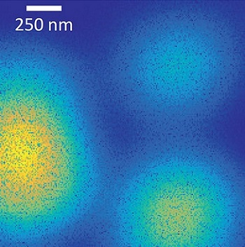
Image of quantum dots in a semiconductor: whereas the image taken with a normal microscope is blurry (left), the new method (right) clearly shows four quantum dots (bright yellow spots). (Image: University of Basel, Department of Physics)
Switched on and off
In recent years, however, scientists have managed to get around this resolution limit and generate images of structures measuring just a few nanometers across. To do so, they used lasers of various wavelengths to trigger fluorescence in molecules in part of the substance while suppressing it in the surrounding areas. This allows them to image structures such as dye molecules, which are just a few nanometers in size. The development of this method (Stimulated Emission Depletion, STED) was honored with the Nobel Prize in Chemistry 2014.
For all objects with two energy levels
Timo Kaldewey, from Professor Richard Warburton’s team at the University of Basel’s Department of Physics and Swiss Nanoscience Institute, has now worked with colleagues at Ruhr-University Bochum (Germany) to develop a similar technique that allows the imaging of nanoscale objects, particularly a quantum mechanical two-level system.
The physicists studied what are known as quantum dots, artificial atoms in a semiconductor, which the new method was able to image as bright spots. The scientists excited the atoms with a pulsed laser, which changes its color during each pulse. As a result, the atom’s fluorescence is switched on and off.
Whereas the STED method only works by occupying at least four different energy levels in response to the laser excitation, the new method from Basel also works with atoms that have just two energy states. Two-state systems of this kind constitute important model systems for quantum mechanics.
Unlike STED microscopy, the new method also releases no heat. “This is a huge advantage, as any heat released can destroy the molecules you’re examining,” explains Richard Warburton. “Our nanoscope is suitable for all objects with two energy levels, such as real atoms, cold molecules, quantum dots, or color centers.”
The project received funding from, among other sources, the National Center of Competence in Research “Quantum Science and Technology” (NCCR QSIT), the Swiss National Science Foundation, and the European Union under the FP7 program.
Share on:


Testimonial
"In a year when every marketing dollar mattered, I chose to keep I-Connect007 in our 2025 plan. Their commitment to high-quality, insightful content aligns with Koh Young’s values and helps readers navigate a changing industry. "
Brent Fischthal - Koh YoungSuggested Items
MEMS & Imaging Sensors Summit to Spotlight Sensing Revolution for Europe’s Leadership
09/11/2025 | SEMIIndustry experts will gather November 19-20 at the SEMI MEMS & Imaging Sensors Summit 2025 to explore the latest breakthroughs in AI-driven MEMS and imaging optimization, AR/VR technologies, and advanced sensor solutions for critical defence applications.
Direct Imaging System Market Size to Hit $4.30B by 2032, Driven by Increasing Demand for High-Precision PCB Manufacturing
09/11/2025 | Globe NewswireAccording to the SNS Insider, “The Direct Imaging System Market size was valued at $2.21 Billion in 2024 and is projected to reach $4.30 Billion by 2032, growing at a CAGR of 8.68% during 2025-2032.”
I-Connect007’s Editor’s Choice: Five Must-Reads for the Week
07/04/2025 | Marcy LaRont, I-Connect007For our industry, we have seen several bullish market announcements over the past few weeks, including one this week by IDC on the massive growth in the global server market. We’re also closely watching global trade and nearshoring. One good example of successful nearshoring is Rehm Thermal Systems, which celebrates its 10th anniversary in Mexico and the official opening of its new building in Guadalajara.
Driving Innovation: Direct Imaging vs. Conventional Exposure
07/01/2025 | Simon Khesin -- Column: Driving InnovationMy first camera used Kodak film. I even experimented with developing photos in the bathroom, though I usually dropped the film off at a Kodak center and received the prints two weeks later, only to discover that some images were out of focus or poorly framed. Today, every smartphone contains a high-quality camera capable of producing stunning images instantly.
United Electronics Corporation Advances Manufacturing Capabilities with Schmoll MDI-ST Imaging Equipment
06/24/2025 | United Electronics CorporationUnited Electronics Corporation has successfully installed the advanced Schmoll MDI-ST (XL) imaging equipment at their advanced printed circuit board facility. This significant technology investment represents a continued commitment to delivering superior products and maintaining their position as an industry leader in precision PCB manufacturing.