


 Trouble in Your Tank: Implementing Direct Metallization in Advanced Substrate Packaging
 It’s Only Common Sense: Storytelling That Sells—Stop Pitching, Start Painting Pictures
 The Right Approach: Get Ready for ISO 9001 Version 6


Study Reveals Secrets of ‘Fluid-like’ Heat Flow in Solid Semiconductor at Nanoscale
February 1, 2018 | Purdue UniversityEstimated reading time: 3 minutes
Researchers are applying the same “hydrodynamic transport model” used to study flow in fluids to explain heat transport in a solid semiconductor, with potential implications for the design of high-speed transistors and lasers.
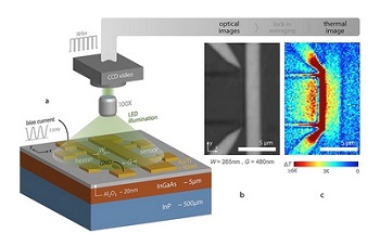
Image caption: Purdue University researchers have visualized temperature changes produced by ultra-small heat sources, gold strips formed on top of the semiconductor indium gallium arsenide. The work has potential implications for the design of high-speed transistors and lasers. This image (a) depicts the device structure and experimental setup, an optical image (b) of the fabricated device and (c) an experimental thermal image. (Purdue University image/Amirkoushyar Ziabari, Bjorn Vermeersch)
Thermal imaging of tiny nanoscale semiconductor heat sources revealed details about vortices of heat-carrying objects called phonons.
The new findings have potentially important implications for “thermal crosstalk,” in which multiple heat sources next to each other impact the overall temperature of the system, hindering performance. The researchers used a technique called full-field thermoreflectance thermal imaging to directly visualize temperature changes produced by ultra-small heat sources, gold strips formed on top of the semiconductor indium gallium arsenide.
The research concerns the crucial role of phonons, quantum-mechanical objects, or “quasiparticles,” that describe how vibrations travel through a material's crystal structure. The phonons are said to be “heat carriers” in solid materials.
“This is the first time such hydrodynamic effects are indirectly observed for heat propagation in a solid,” said Ali Shakouri, Purdue University's Mary Jo and Robert L. Kirk Director of the Birck Nanotechnology Center and a professor of electrical and computer engineering. “While structures called vortices are common in fluid flows such as water or air, this is the first time we’ve seen that they can be present inside solids for phonon flow in the typical semiconductor indium gallium arsenide, which is used in high-speed transistors and lasers.”
“The observed thermal crosstalk reduction has important implications in the design of nanoscale electronic and optoelectronic devices,” said Purdue postdoctoral research associate Amirkoushyar Ziabari, the paper’s lead author. “As the size of electronic and optoelectronic devices are getting smaller, there are more and more devices being packed into a smaller area, so the thermal crosstalk between these devices becomes important. Knowing the accurate thermal behavior in the neighborhood and a few microns from heat sources would help design better state-of-the-art devices in terms of performance, speed, thermal reliability, and so on.”
The researchers found that the reduced thermal crosstalk is caused by vortices generated near the edge of the heat sources.
“This is similar to the vortices that are observed at the edge of an obstacle placed inside of a current of air or water, such as behind an airplane wing,” Shakouri said.
The governing law of heat conduction, known as the Fourier Law or the heat-diffusion equation, does not accurately predict thermal transport for devices on the nanoscale. Because the Fourier diffusion equation doesn't explain the heat transport at those scales, this transport regime is called non-diffusive.
“As the size of electronic and optoelectronic devices are getting smaller, it is important to consider this non-diffusive behavior for design and optimization of such small devices,” Ziabari said. “These new measurements show that at nanoscales, heat propagation has interesting ‘fluid-like’ behavior.”
Conventional methods do not account for vortices of heat transport found at the nanoscale.
“Vorticity only becomes important when the characteristic source dimension is comparable to the hydrodynamic length scale of about 150 nanometers,” he said.
The Fourier theory substantially overestimates the experimentally observed temperature a short distance away from the heater lines.
“The surprising effect was that the temperature decays much faster than what Fourier theory predicted,” Shakouri said. “Within a distance of 1 or 2 microns of a small heat source - a line about 100 nanometers wide - temperature could be one-third to one-fourth what Fourier theory predicts.”
The thermoreflectance thermal imaging approach allows researchers to create maps of temperature rise at far higher resolution than otherwise possible using light in the visible range.
The work was performed by researchers at the Birck Nanotechnology Center in Purdue’s Discovery Park, Purdue’s School of Electrical and Computer Engineering, Universitat Autónoma de Barcelona, Commissariat à l’Énergie Atomique in Grenoble, France, and the Department of Mechanical and Materials Engineering at the University of Cincinnati. All co-authors are listed in the abstract.
The research was partially funded by the European Commission and the Spanish Ministry of Economy and Competitiveness.
Share on:


Testimonial
"Advertising in PCB007 Magazine has been a great way to showcase our bare board testers to the right audience. The I-Connect007 team makes the process smooth and professional. We’re proud to be featured in such a trusted publication."
Klaus Koziol - atgSuggested Items
ASM Technologies Limited signs MoU with the Guidance, Government of Tamilnadu to Expand Design-Led Manufacturing capabilities for ESDM
09/15/2025 | ASM TechnologiesASM Technologies Limited, a pioneer in Design- Led Manufacturing in the semiconductor and automotive industries, announced signing of Memorandum of Understanding (MoU) with the Guidance, Government of Tamilnadu whereby it will invest Rs. 250 crores in the state to expand its ESDM related Design-Led Manufacturing and precision engineering capacity. ASM Technologies will acquire 5 acres of land from the Government of Tamilnadu to set up a state-of-the-art design facility in Tamil Nadu's growing technology manufacturing ecosystem, providing a strong strategic advantage and long-term benefits for ASM.
Variosystems Strengthens North American Presence with Southlake Relaunch 2025
09/15/2025 | VariosystemsVariosystems celebrated the relaunch of its U.S. facility in Southlake, Texas. After months of redesign and reorganization, the opening marked more than just the return to a modernized production site—it was a moment to reconnect with our teams, partners, and the local community.
Deca, Silicon Storage Technology Announce Strategic Collaboration to Enable NVM Chiplet Solutions
09/11/2025 | Microchip Technology Inc.As traditional monolithic chip designs grow in complexity and increase in cost, the interest and adoption of chiplet technology in the semiconductor industry also increases.
I-Connect007 Launches New Podcast Series on Ultra High Density Interconnect (UHDI)
09/10/2025 | I-Connect007I-Connect007 is excited to announce the debut of its latest podcast series, which shines a spotlight on one of the most important emerging innovations in electronics manufacturing: Ultra-High-Density Interconnect (UHDI). The series kicks off with Episode One, “Ultra HDI: What does it mean to people? Why would they want it?” Host Nolan Johnson is joined by guest expert John Johnson, Director of Quality and Advanced Technology at American Standard Circuits (ASC).
Global Citizenship: Together for a Perfect PCB Solution
09/10/2025 | Tom Yang -- Column: Global CitizenshipIf there’s one thing we’ve learned in the past few decades of electronics evolution, it’s that no region has a monopoly on excellence. Whether it’s materials science breakthroughs in Europe, manufacturing efficiencies in China, or design innovations in Silicon Valley, the PCB industry thrives on collaboration.