


 Trouble in Your Tank: Implementing Direct Metallization in Advanced Substrate Packaging
 It’s Only Common Sense: Storytelling That Sells—Stop Pitching, Start Painting Pictures
 The Right Approach: Get Ready for ISO 9001 Version 6


New UC Riverside Research Advances Spintronics Technology
February 2, 2018 | University of California, RiversideEstimated reading time: 4 minutes
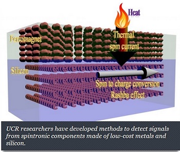
Engineers at the University of California, Riverside, have reported advances in so-called “spintronic” devices that will help lead to a new technology for computing and data storage. They have developed methods to detect signals from spintronic components made of low-cost metals and silicon, which overcomes a major barrier to wide application of spintronics. Previously such devices depended on complex structures that used rare and expensive metals such as platinum. The researchers were led by Sandeep Kumar, an assistant professor of mechanical engineering.
Spintronic devices promise to solve major problems in today’s electronic computers, in that the computers use massive amounts of electricity and generate heat that requires expending even more energy for cooling. By contrast, spintronic devices generate little heat and use relatively minuscule amounts of electricity. Spintronic computers would require no energy to maintain data in memory. They would also start instantly and have the potential to be far more powerful than today’s computers.
While electronics depends on the charge of electrons to generate the binary ones or zeroes of computer data, spintronics depends on the property of electrons called spin. Spintronic materials register binary data via the “up” or “down” spin orientation of electrons—like the north and south of bar magnets—in the materials. A major barrier to development of spintronics devices is generating and detecting the infinitesimal electric spin signals in spintronic materials.
In one paper published in the January issue of the scientific journal Applied Physics Letters, Kumar and colleagues reported an efficient technique of detecting the spin currents in a simple two-layer sandwich of silicon and a nickel-iron alloy called Permalloy. All three of the components are both inexpensive and abundant and could provide the basis for commercial spintronic devices. They also operate at room temperature. The layers were created with the widely used electronics manufacturing processes called sputtering. Co-authors of the paper were graduate students Ravindra Bhardwaj and Paul Lou.
In their experiments, the researchers heated one side of the Permalloy-silicon bi-layer sandwich to create a temperature gradient, which generated an electrical voltage in the bi-layer. The voltage was due to phenomenon known as the spin-Seebeck effect. The engineers found that they could detect the resulting “spin current” in the bi-layer due to another phenomenon known as the “inverse spin-Hall effect.”
The researchers said their findings will have application to efficient magnetic switching in computer memories, and “these scientific breakthroughs may give impetus” to development of such devices. More broadly, they concluded, “These results bring the ubiquitous Si (silicon) to forefront of spintronics research and will lay the foundation of energy efficient Si spintronics and Si spin caloritronics devices.”
In two other scientific papers, the researchers demonstrated that they could generate a key property for spintronics materials, called antiferromagnetism, in silicon. The achievement opens an important pathway to commercial spintronics, said the researchers, given that silicon is inexpensive and can be manufactured using a mature technology with a long history of application in electronics.
Ferromagnetism is the property of magnetic materials in which the magnetic poles of the atoms are aligned in the same direction. In contrast, antiferromagnetism is a property in which the neighboring atoms are magnetically oriented in opposite directions. These “magnetic moments” are due to the spin of electrons in the atoms, and is central to the application of the materials in spintronics.
In the two papers, Kumar and Lou reported detecting antiferromagnetism in the two types of silicon—called n-type and p-type—used in transistors and other electronic components. N-type semiconductor silicon is “doped” with substances that cause it to have an abundance of negatively-charged electrons; and p-type silicon is doped to have a large concentration of positively charged “holes.” Combining the two types enables switching of current in such devices as transistors used in computer memories and other electronics.
In the paper in the Journal of Magnetism and Magnetic Materials, Lou and Kumar reported detecting the spin-Hall effect and antiferromagnetism in n-silicon. Their experiments used a multilayer thin film comprising palladium, nickel-iron Permalloy, manganese oxide and n-silicon.
And in the second paper, in the scientific journal physica status solidi, they reported detecting in p-silicon spin-driven antiferromagnetism and a transition of silicon between metal and insulator properties. Those experiments used a thin film similar to those with the n-silicon.
The researchers wrote in the latter paper that “The observed emergent antiferromagnetic behavior may lay the foundation of Si (silicon) spintronics and may change every field involving Si thin films. These experiments also present potential electric control of magnetic behavior using simple semiconductor electronics physics. The observed large change in resistance and doping dependence of phase transformation encourages the development of antiferromagnetic and phase change spintronics devices.”
In further studies, Kumar and his colleagues are developing technology to switch spin currents on and off in the materials, with the ultimate goal of creating a spin transistor. They are also working to generate larger, higher-voltage spintronic chips. The result of their work could be extremely low-power, compact transmitters and sensors, as well as energy-efficient data storage and computer memories, said Kumar.
Share on:


Testimonial
"We’re proud to call I-Connect007 a trusted partner. Their innovative approach and industry insight made our podcast collaboration a success by connecting us with the right audience and delivering real results."
Julia McCaffrey - NCAB GroupSuggested Items
September PCB007 Magazine: The Future of Advanced Materials
09/16/2025 | I-Connect007 Editorial TeamMoore’s Law is no more, and the advanced material solutions being developed to grapple with this reality are surprising, stunning, and perhaps a bit daunting. Buckle up for a dive into advanced materials and a glimpse into the next chapters of electronics manufacturing.
I-Connect007 Launches Advanced Electronics Packaging Digest
09/15/2025 | I-Connect007I-Connect007 is pleased to announce the launch of Advanced Electronics Packaging Digest (AEPD), a new monthly digital newsletter dedicated to one of the most critical and rapidly evolving areas of electronics manufacturing: advanced packaging at the interconnect level.
Panasonic Industry will Double the Production Capacity of MEGTRON Multi-layer Circuit Board Materials Over the Next Five Years
09/15/2025 | Panasonic Industry Co., Ltd.Panasonic Industry Co., Ltd., a Panasonic Group company, announced plans for a major expansion of its global production capacity for MEGTRON multi-layer circuit board materials today. The company plans to double its production over the next five years to meet growing demand in the AI server and ICT infrastructure markets.
Trouble in Your Tank: Implementing Direct Metallization in Advanced Substrate Packaging
09/15/2025 | Michael Carano -- Column: Trouble in Your TankDirect metallization systems based on conductive graphite are gaining popularity throughout the world. The environmental and productivity gains achievable with this process are outstanding. Direct metallization reduces the costs of compliance, waste treatment, and legal issues related to chemical exposure. A graphite-based direct plate system has been devised to address these needs.
Fresh PCB Concepts: Designing for Success at the Rigid-flex Transition Area
08/28/2025 | Team NCAB -- Column: Fresh PCB ConceptsRigid-flex PCBs come in all shapes and sizes. Manufacturers typically use fire-retardant, grade 4 (FR-4) materials in the rigid section and flexible polyimide materials in the flex region. Because of the small size, some rigid-flex PCBs, like those for hearing aid devices, are among the most challenging to manufacture. However, regardless of its size, we should not neglect the transition area between the rigid and flexible material.