


 Trouble in Your Tank: Implementing Direct Metallization in Advanced Substrate Packaging
 It’s Only Common Sense: Storytelling That Sells—Stop Pitching, Start Painting Pictures
 The Right Approach: Get Ready for ISO 9001 Version 6


Measuring the Temperature of Two-Dimensional Materials at the Atomic Level
February 5, 2018 | University of Illinois at ChicagoEstimated reading time: 3 minutes
Researchers at the University of Illinois at Chicago describe a new technique for precisely measuring the temperature and behavior of new two-dimensional materials that will allow engineers to design smaller and faster microprocessors.
Newly developed two-dimensional materials, such as graphene — which consists of a single layer of carbon atoms — have the potential to replace traditional microprocessing chips based on silicon, which have reached the limit of how small they can get. But engineers have been stymied by the inability to measure how temperature will affect these new materials, collectively known as transition metal dichalcogenides, or TMDs.
Using scanning transmission electron microscopy combined with spectroscopy, researchers at UIC were able to measure the temperature of several two-dimensional materials at the atomic level, paving the way for much smaller and faster microprocessors. They were also able to use their technique to measure how the two-dimensional materials would expand when heated.
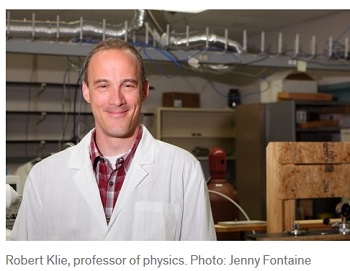
“Microprocessing chips in computers and other electronics get very hot, and we need to be able to measure not only how hot they can get, but how much the material will expand when heated,” said Robert Klie, professor of physics at UIC and corresponding author of the paper. “Knowing how a material will expand is important because if a material expands too much, connections with other materials, such as metal wires, can break and the chip is useless.”
Traditional ways to measure temperature don’t work on tiny flakes of two-dimensional materials that would be used in microprocessors because they are just too small. Optical temperature measurements, which use a reflected laser light to measure temperature, can’t be used on TMD chips because they don’t have enough surface area to accommodate the laser beam.
“We need to understand how heat builds up and how it is transmitted at the interface between two materials in order to build efficient microprocessors that work,” said Klie.
Klie and his colleagues devised a way to take temperature measurements of TMDs at the atomic level using scanning transition electron microscopy, which uses a beam of electrons transmitted through a specimen to form an image.
“Using this technique, we can zero in on and measure the vibration of atoms and electrons, which is essentially the temperature of a single atom in a two-dimensional material,” said Klie. Temperature is a measure of the average kinetic energy of the random motions of the particles, or atoms that make up a material. As a material gets hotter, the frequency of the atomic vibration gets higher. At absolute zero, the lowest theoretical temperature, all atomic motion stops.
Klie and his colleagues heated microscopic “flakes” of various TMDs inside the chamber of a scanning transmission electron microscope to different temperatures and then aimed the microscope’s electron beam at the material. Using a technique called electron energy-loss spectroscopy, they were able to measure the scattering of electrons off the two-dimensional materials caused by the electron beam. The scattering patterns were entered into a computer model that translated them into measurements of the vibrations of the atoms in the material – in other words, the temperature of the material at the atomic level.
“With this new technique, we can measure the temperature of a material with a resolution that is nearly 10 times better than conventional methods,” said Klie. “With this new approach, we can design better electronic devices that will be less prone to overheating and consume less power.”
The technique can also be used to predict how much materials will expand when heated and contract when cooled, which will help engineers build chips that are less prone to breaking at points where one material touches another, such as when a two-dimensional material chip makes contact with a wire.
“No other method can measure this effect at the spatial resolution we report,” said Klie. “This will allow engineers to design devices that can manage temperature changes between two different materials at the nano-scale level.”
Xuan Hu, Poya Yasaei, Jacob Jokisaari, Serdar Ogut and Amin Salehi-Khojin of the University of Illinois at Chicago, are co-authors of the paper.
This research was supported by EFRI 2-DARE grant 1542864 from the National Science Foundation.
Share on:


Testimonial
"The I-Connect007 team is outstanding—kind, responsive, and a true marketing partner. Their design team created fresh, eye-catching ads, and their editorial support polished our content to let our brand shine. Thank you all! "
Sweeney Ng - CEE PCBSuggested Items
I-Connect007 Launches Advanced Electronics Packaging Digest
09/15/2025 | I-Connect007I-Connect007 is pleased to announce the launch of Advanced Electronics Packaging Digest (AEPD), a new monthly digital newsletter dedicated to one of the most critical and rapidly evolving areas of electronics manufacturing: advanced packaging at the interconnect level.
Panasonic Industry will Double the Production Capacity of MEGTRON Multi-layer Circuit Board Materials Over the Next Five Years
09/15/2025 | Panasonic Industry Co., Ltd.Panasonic Industry Co., Ltd., a Panasonic Group company, announced plans for a major expansion of its global production capacity for MEGTRON multi-layer circuit board materials today. The company plans to double its production over the next five years to meet growing demand in the AI server and ICT infrastructure markets.
Trouble in Your Tank: Implementing Direct Metallization in Advanced Substrate Packaging
09/15/2025 | Michael Carano -- Column: Trouble in Your TankDirect metallization systems based on conductive graphite are gaining popularity throughout the world. The environmental and productivity gains achievable with this process are outstanding. Direct metallization reduces the costs of compliance, waste treatment, and legal issues related to chemical exposure. A graphite-based direct plate system has been devised to address these needs.
Fresh PCB Concepts: Designing for Success at the Rigid-flex Transition Area
08/28/2025 | Team NCAB -- Column: Fresh PCB ConceptsRigid-flex PCBs come in all shapes and sizes. Manufacturers typically use fire-retardant, grade 4 (FR-4) materials in the rigid section and flexible polyimide materials in the flex region. Because of the small size, some rigid-flex PCBs, like those for hearing aid devices, are among the most challenging to manufacture. However, regardless of its size, we should not neglect the transition area between the rigid and flexible material.
Global Sourcing Spotlight: How to Evaluate Supplier Capabilities Worldwide
08/20/2025 | Bob Duke -- Column: Global Sourcing SpotlightIn global sourcing, the difference between a competitive edge and a catastrophic disruption often comes down to how well you vet your suppliers. Sourcing advanced PCBs, precision components, or materials for complex assemblies demands diligence, skepticism, and more than a little time on airplanes. Here’s how to do your due diligence when evaluating international suppliers and why cutting corners can cost you more than money.