


 Trouble in Your Tank: Implementing Direct Metallization in Advanced Substrate Packaging
 It’s Only Common Sense: Storytelling That Sells—Stop Pitching, Start Painting Pictures
 The Right Approach: Get Ready for ISO 9001 Version 6


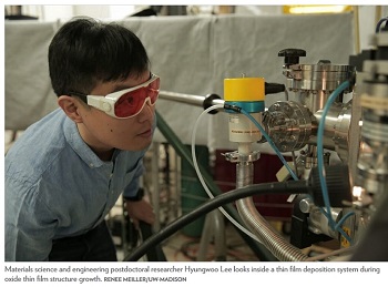
Beyond Silicon: Researchers Solve a Materials Mystery Key to Next-Generation Electronic Devices
February 6, 2018 | University of Wisconsin-MadisonEstimated reading time: 2 minutes
Lennon and McCartney. Abbott and Costello. Peanut butter and jelly.
Think of one half of any famous duo, and the other half likely comes to mind. Not only do they complement each other, but together they work better.
The same is true in the burgeoning field of oxide electronics materials. Boasting a wide array of behaviors, including electronic, magnetic and superconducting, these multifunctional materials are poised to expand the way we think about the functions of traditional silicon-based electronic devices such as cell phones or computers.
Yet until now, a critical aspect has been missing — one that complements the function of electrons in oxide electronics. And a team led by University of Wisconsin–Madison materials scientist Chang-Beom Eom has directly observed that missing second half of the duo necessary to move oxide electronics materials forward.
It’s called a two-dimensional hole gas — a counterpart to something known as a two-dimensional electron gas. For more than a decade, researchers have recognized a hole gas appearance was possible, but haven’t been able to create it experimentally.
“The 2D hole gas was not possible primarily because perfect-enough crystals could not be grown,” says Eom, the Theodore H. Geballe Professor and Harvey D. Spangler Distinguished Professor of materials science and engineering. “Inside, there were defects that killed the hole gas.”
Eom is a world expert in material growth, using techniques that allow him to meticulously build, or “grow,” each layer of a material with atomic precision. That expertise, combined with insight into the interaction between layers in their structure, was key in identifying the elusive 2D hole gas.
“We were able to design the correct structure and make near-perfect crystals, all without defects that degrade the hole gas,” he says.
Also important in identifying the hole gas was the almost-symmetrical way in which Eom assembled the various layers — something like a club sandwich. While other researchers have made the material in a bi-layer structure, Eom designed a triple layer. He alternated layers of strontium oxide and titanium dioxide on the bottom, then layers of lanthanum oxide and aluminum oxide, then added additional layers of strontium oxide and titanium dioxide on the top.
As a result, the hole gas forms at the interface of the layers on the top, while the electron gas forms at the interface of the layers on the bottom — the first demonstration of a very powerful complementary pair.
Just as people 50 years ago likely could not have envisioned communicating via wireless devices, the advance sets forth a platform that can enable new concepts-applications that today remain beyond our wildest dreams.
“We’re not just improving the performance of devices,” says Eom. “So, not improving a cell phone, for example — but envisioning an entirely new device made possible by this advance. This is the beginning of an exciting new path.”
Eom’s collaborators from UW–Madison include physics professor Mark Rzchowski and graduate students in materials science and engineering and physics, as well as collaborators from The Ohio State University, the University of Nebraska at Lincoln, Argonne National Laboratory, and Sungkyunkwan University and Pohang University of Science and Technology in Korea.
Share on:


Testimonial
"Our marketing partnership with I-Connect007 is already delivering. Just a day after our press release went live, we received a direct inquiry about our updated products!"
Rachael Temple - AlltematedSuggested Items
Beyond the Board: What Companies Need to Know Before Entering the MilAero PCB Market
09/16/2025 | Jesse Vaughan -- Column: Beyond the BoardThe MilAero electronics supply chain offers opportunities for manufacturers that are both prestigious and strategically important. Serving prime contractors and Tier-1 suppliers can mean long-term program stability and the satisfaction of contributing to national security. At the same time, this sector is unlike commercial electronics in almost every respect. Success requires more than technical capabilities, it requires patience, preparation, attention to detail, and a clear understanding of how the business model differs.
India’s Aerospace and Defence Engineered for Power, Driven by Electronics
09/16/2025 | Gaurab Majumdar, Global Electronics AssociationWith a defence budget of $82.05 billion (2025–26) and a massive $223 billion earmarked for aerospace and defence spending over the next decade, India is rapidly positioning itself as a major player in the global defence and aerospace market.
I-Connect007 Launches Advanced Electronics Packaging Digest
09/15/2025 | I-Connect007I-Connect007 is pleased to announce the launch of Advanced Electronics Packaging Digest (AEPD), a new monthly digital newsletter dedicated to one of the most critical and rapidly evolving areas of electronics manufacturing: advanced packaging at the interconnect level.
Global Interposer Market to Surge Nearly Fivefold by 2034
09/15/2025 | I-Connect007 Editorial TeamRevenue for the global interposer market is projected to climb from $471 million in 2025 to more than $2.3 billion by 2034, according to a new report from Business Research Insights. The growth represents a CAGR of nearly 20 percent over the forecast period.
ICAPE Group Unveils Exclusive Report on Sustainability in Electronics Manufacturing
09/15/2025 | ICAPE GroupICAPE Group, a global leader in printed circuit boards (PCBs) and custom electronics manufacturing, today announces the launch of its 2025 Industry Outlook & Innovation Report: Sustainability in Electronics Manufacturing. This exclusive report is accompanied by fresh insights from a dedicated Statista survey of 100 electronics manufacturing professionals, commissioned by ICAPE Group.