


 It’s Only Common Sense: The Importance of Setting Realistic Expectations
 Marcy’s Musings: The Relentless Pursuit of Perfection
 Dan’s Biz Bookshelf: ‘Do/Start'


The Dawn of Gallium Oxide Microelectronics
February 9, 2018 | AIP.orgEstimated reading time: 2 minutes
Silicon has long been the go-to material in the world of microelectronics and semiconductor technology. But silicon still faces limitations, particularly with scalability for power applications. Pushing semiconductor technology to its full potential requires smaller designs at higher energy density.
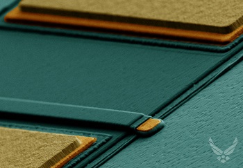
Image caption: A false-color, plan-view SEM image of a lateral gallium oxide field effect transistor with an optically defined gate. From near (bottom) to far (top): the source, gate, and drain electrodes. Metal is shown in yellow and orange, dark blue represents dielectric material, and lighter blue denotes the gallium oxide substrate. CREDIT: AFRL Sensors Directorate at WPAFB, Ohio, U.S.
“One of the largest shortcomings in the world of microelectronics is always good use of power: Designers are always looking to reduce excess power consumption and unnecessary heat generation,” said Gregg Jessen, principal electronics engineer at the Air Force Research Laboratory. “Usually, you would do this by scaling the devices. But the technologies in use today are already scaled close to their limits for the operating voltage desired in many applications. They are limited by their critical electric field strength.”
Transparent conductive oxides are a key emerging material in semiconductor technology, offering the unlikely combination of conductivity and transparency over the visual spectrum. One conductive oxide in particular has unique properties that allow it to function well in power switching: Ga2O3, or gallium oxide, a material with an incredibly large bandgap.
In their article published this week in Applied Physics Letters, from AIP Publishing, authors Masataka Higashiwaki and Jessen outline a case for producing microelectronics using gallium oxide. The authors focus on field effect transistors (FETs), devices that could greatly benefit from gallium oxide’s large critical electric field strength. a quality which Jessen said could enable the design of FETs with smaller geometries and aggressive doping profiles that would destroy any other FET material.
The material’s flexibility for various applications is due to its broad range of possible conductivities -- from highly conductive to very insulating -- and high-breakdown-voltage capabilities due to its electric field strength. Consequently, gallium oxide can be scaled to an extreme degree. Large-area gallium oxide wafers can also be grown from the melt, lowering manufacturing costs.
“The next application for gallium oxide will be unipolar FETs for power supplies,” Jessen said. “Critical field strength is the key metric here, and it results in superior energy density capabilities. The critical field strength of gallium oxide is more than 20 times that of silicon and more than twice that of silicon carbide and gallium nitride.”
The authors discuss manufacturing methods for Ga2O3 wafers, the ability to control electron density, and the challenges with hole transport. Their research suggests that unipolar Ga2O3 devices will dominate. Their paper also details Ga2O3 applications in different types of FETs and how the material can be of service in high-voltage, high-power and power-switching applications.
“From a research perspective, gallium oxide is really exciting,” Jessen said. “We are just beginning to understand the full potential of these devices for several applications, and it’s a great time to be involved in the field.”
Share on:


Suggested Items
Electroninks Acquires Complete UTDots Advanced Materials Nanoinks Portfolio and IP
05/19/2025 | ElectroninksElectroninks, the leader in metal organic decomposition (MOD) inks for additive manufacturing and advanced semiconductor packaging, announced it has officially completed its full acquisition of UTDots products and IP into its portfolio, further expanding its offerings in digital printing for high-performance applications.
Indium to Feature Power Electronics Solutions at SEMICON Southeast Asia 2025
05/19/2025 | Indium CorporationAs a trusted leader in materials science for advanced electronics assembly, Indium Corporation® is proud to showcase its innovative power electronics solutions at SEMICON Southeast Asia 2025, May 20–22, in Marina Bay Sands, Singapore.
MVTec Presents Advantages of Machine Vision for Battery Production
05/16/2025 | MVTecMVTec Software GmbH, a leading international manufacturer of machine vision software, will once again demonstrate the added value of machine vision for battery production at this year's Battery Show Europe in Stuttgart.
DuPont to Introduce Advanced Kalrez Sealing Innovations for Semiconductor Manufacturing at SEMICON Southeast Asia
05/15/2025 | DuPontDuPont is excited to announce its participation in SEMICON Southeast Asia (SEMICON SEA), taking place May 20-22, 2025, in Singapore. At booth L3105,
Facing the Future: The Role of 5G and Beyond in Shaping PCB Demand
05/13/2025 | Prashant Patel -- Column: Facing the FutureInnovations that push the boundaries of connectivity shape the future of technology, processing power, and miniaturization. 5G and emerging 6G technologies are critical in transforming industries from telecommunications and healthcare to autonomous systems. This affects the printed circuit board (PCB) industry, where demand for high-performance, miniaturized, and advanced PCBs is surging. This column explores the key applications of 5G and beyond, the challenges in designing high-frequency PCBs, the effects of miniaturization, industry collaborations, and opportunities for North American companies in this space.