














 The Big Picture: Not One, But Three Grey Rhinos
 It’s Only Common Sense: Make Your ‘Account’ the Whole Organization
 Dan’s Biz Bookshelf: ‘Building a Story Brand 2.0’





Piezoelectrics are one of the world`s most amazing materials. It is possible to literally squeeze electricity from them. That is, an electric charge appears at the time of the material`s compression (or stretching). This is called the piezoelectric effect. Piezoelectric materials can be applied in many fields — from pressure sensors and sensitive elements of a microphone to the controller ink pressing in ink-jet printers and quartz resonators.
Lead zirconate titanate is one of the most popular piezoelectric materials. However, it has several disadvantages: it is heavy and inflexible. Additionally, lead production often causes great harm to the environment. That is why scientists are constantly looking for new materials with low lead content as well as with less weight and greater flexibility. In particular, the creation of flexible piezoelectric materials (while maintaining the key properties) would greatly expand piezoelectric materials` possibilities both as acoustic membrane and as pressure sensors.
An international team of scientists from the University of Duisburg-Essen (Germany), NUST MISIS, National Research Tomsk State University and the National Research University of Electronic Technology, working with the financial support of the Russian Science Foundation (grant 16-19-10112), has managed to create such a material and analyze its properties. For this, the nanoparticles consisting of titanate-zicronate barium-lead were placed in a complex polymer consisting of vinylidene disluoride and trifluoroethylene. By diversifying the composition of the components, scientists were able to get the most ideal composite.
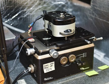
“The Russian-German group of scientists, including Dmitri Kiselev, a Senior Researcher at the NUST MISIS R&D Center for Materials Science & Metallurgy, has managed to create a composite material based on ceramics and organic polymer whose properties exceed today`s best piezoelectric materials. The research’s experimental part was carried out with an atomic-force microscope in the University of Duisburg-Essen (Germany). Thanks to this scientific collaboration, Dmitri Kiselev has gained skills from the world`s best scanning probe microscope, which he can later apply at NUST MISIS”, said Alevtina Chernikova, Rector of NUST MISIS.
According to Dmitri Kiselev, the developed material has a very distinct field of application due to its polymer component: “Composite materials based on polymer and classic ferroelectrics, which have piezo- and pyroelectric properties, have a number of advantages compared to pure ceramics: low density, the ability to manufacture parts of any size and shape, mechanical elasticity, stability of electrophysical properties, and the simplicity and relatively low cost of production. Additionally, the synthesized composite has proved to be excellent at high pressures which makes it an excellent base for pressure sensors”.
According to Kiselev, to study the composite they had to modify the standard technique which allowed them to correctly visualize the nanoparticles of ceramics in the volume of the polymer matrix: “In order to capture the electrical signal more clearly, we heated our sample in a certain way from room temperature to 60 degrees Celsius. It allowed us to measure the material’s characteristics very qualitatively and reproducibly. Our method will greatly simplify the work of our colleagues in the study of composites, so I hope that it will be in demand among our colleagues microscopists”.
“It is now easier for Russian scientists to carry out world-class measurements as the MFP 3D Stand Аlone (Asylum Research) microscope is now available at the NUST MISIS Center for Collaborative Use, hence why we are now actively collaborating with several institutes from the Russian Academy of Sciences as well as other Moscow universities”, Kiselev concluded.


