


 Trouble in Your Tank: Implementing Direct Metallization in Advanced Substrate Packaging
 It’s Only Common Sense: Storytelling That Sells—Stop Pitching, Start Painting Pictures
 The Right Approach: Get Ready for ISO 9001 Version 6


Reinventing the Inductor
February 22, 2018 | University of California - Santa BarbaraEstimated reading time: 3 minutes
A basic building block of modern technology, inductors are everywhere: cellphones, laptops, radios, televisions, cars. And surprisingly, they are essentially the same today as in 1831, when they were first created by English scientist Michael Faraday.
The particularly large size of inductors made according to Faraday’s design are a limiting factor in delivering the miniaturized devices that will help realize the potential of the Internet of Things, which promises to connect people to some 50 billion objects by 2020. That lofty goal is expected to have an estimated economic impact between $2.7 and $6.2 trillion annually by 2025.
Now, a team at UC Santa Barbara, led by Kaustav Banerjee, a professor in the Department of Electrical and Computer Engineering, has taken a materials-based approach to reinventing this fundamental component of modern electronics. The findings appear in the journal Nature Electronics.
Banerjee and his UCSB team — lead author Jiahao Kang, Junkai Jiang, Xuejun Xie, Jae Hwan Chu and Wei Liu, all members of his Nanoelectronics Research Lab — worked with colleagues from Shibaura Institute of Technology in Japan and Shanghai Jiao Tong University in China to exploit the phenomenon of kinetic inductance to demonstrate a fundamentally different kind of inductor.
All inductors generate both magnetic and kinetic inductance, but in typical metal conductors, the kinetic inductance is so small as to be unnoticeable. “The theory of kinetic inductance has long been known in condensed-matter physics, but nobody ever used it for inductors, because in conventional metallic conductors, kinetic inductance is negligible,” Banerjee explained.
Unlike magnetic inductance, kinetic inductance does not depend on the surface area of the inductor. Rather, kinetic inductance resists current fluctuations that alter the velocity of the electrons, and the electrons resist such change according to Newton’s law of inertia.
Historically, as the technology of transistors and interconnects that link them has advanced, the elements have become smaller. But the inductor, which in its simplest form is a metallic coil wound around a core material, has been the exception.
“On-chip inductors based on magnetic inductance cannot be made smaller in the same way transistors or interconnects scale, because you need a certain amount of surface area to get a certain magnetic flux or inductance value,” explained lead author Kang, who recently completed his Ph.D. under Banerjee’s supervision.
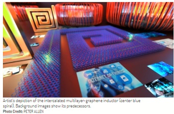
The UCSB team designed a new kind of spiral inductor comprised of multiple layers of graphene. Single-layer graphene exhibits a linear electronic band structure and a correspondingly large momentum relaxation time (MRT) — a few picoseconds or higher compared to that of conventional metallic conductors (like copper used in traditional on-chip inductors), which ranges from 1/1000 to 1/100 of a picosecond. But single-layer graphene has too much resistance for application on an inductor.
However, multilayer graphene offers a partial solution by providing lower resistance, but interlayer couplings cause its MRT to be insufficiently small. The researchers overcame that dilemma with a unique solution: They chemically inserted bromine atoms between the graphene layers — a process called intercalation — that not only further reduced resistance but also separated the graphene layers just enough to essentially decouple them, extending the MRT and thereby increasing kinetic inductance.
The revolutionary inductor, which works in the 10-50 GHz range, offers one-and-a-half times the inductance density of a traditional inductor, leading to a one-third reduction in area while also providing extremely high efficiency. Previously, high inductance and reduced size had been an elusive combination.
“There is plenty of room to increase the inductance density further by increasing the efficiency of the intercalation process, which we are now exploring,” said co-author Jiang.
“We essentially engineered a new nanomaterial to bring forward the previously ‘hidden physics’ of kinetic inductance at room temperature and in a range of operating frequencies targeted for next-generation wireless communications,” Banerjee added.
While Faraday’s version of the inductor proved crucial for practical large scale use of electricity for power and telegraph communication, Banerjee’s version could pave the way for next-generation communications, sensing and energy storage for smarter living.
Share on:


Testimonial
"In a year when every marketing dollar mattered, I chose to keep I-Connect007 in our 2025 plan. Their commitment to high-quality, insightful content aligns with Koh Young’s values and helps readers navigate a changing industry. "
Brent Fischthal - Koh YoungSuggested Items
Trouble in Your Tank: Implementing Direct Metallization in Advanced Substrate Packaging
09/15/2025 | Michael Carano -- Column: Trouble in Your TankDirect metallization systems based on conductive graphite are gaining popularity throughout the world. The environmental and productivity gains achievable with this process are outstanding. Direct metallization reduces the costs of compliance, waste treatment, and legal issues related to chemical exposure. A graphite-based direct plate system has been devised to address these needs.
Closing the Loop on PCB Etching Waste
09/09/2025 | Shawn Stone, IECAs the PCB industry continues its push toward greener, more cost-efficient operations, Sigma Engineering’s Mecer System offers a comprehensive solution to two of the industry’s most persistent pain points: etchant consumption and rinse water waste. Designed as a modular, fully automated platform, the Mecer System regenerates spent copper etchants—both alkaline and acidic—and simultaneously recycles rinse water, transforming a traditionally linear chemical process into a closed-loop system.
Driving Innovation: Depth Routing Processes—Achieving Unparalleled Precision in Complex PCBs
09/08/2025 | Kurt Palmer -- Column: Driving InnovationIn PCB manufacturing, the demand for increasingly complex and miniaturized designs continually pushes the boundaries of traditional fabrication methods, including depth routing. Success in these applications demands not only on robust machinery but also sophisticated control functions. PCB manufacturers rely on advanced machine features and process methodologies to meet their precise depth routing goals. Here, I’ll explore some crucial functions that empower manufacturers to master complex depth routing challenges.
Trouble in Your Tank: Minimizing Small-via Defects for High-reliability PCBs
08/27/2025 | Michael Carano -- Column: Trouble in Your TankTo quote the comedian Stephen Wright, “If at first you don’t succeed, then skydiving is not for you.” That can be the battle cry when you find that only small-diameter vias are exhibiting voids. Why are small holes more prone to voids than larger vias when processed through electroless copper? There are several reasons.
The Government Circuit: Navigating New Trade Headwinds and New Partnerships
08/25/2025 | Chris Mitchell -- Column: The Government CircuitAs global trade winds continue to howl, the electronics manufacturing industry finds itself at a critical juncture. After months of warnings, the U.S. Government has implemented a broad array of tariff increases, with fresh duties hitting copper-based products, semiconductors, and imports from many nations. On the positive side, tentative trade agreements with Europe, China, Japan, and other nations are providing at least some clarity and counterbalance.