


 Trouble in Your Tank: Implementing Direct Metallization in Advanced Substrate Packaging
 It’s Only Common Sense: Storytelling That Sells—Stop Pitching, Start Painting Pictures
 The Right Approach: Get Ready for ISO 9001 Version 6


Splitting Crystals for 2D Metallic Conductivity
February 22, 2018 | Tohoku UniversityEstimated reading time: 2 minutes
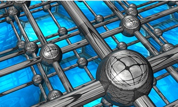
Adding oxygen atoms to a perovskite-like crystal material splits it into layers, giving it unique electrical properties.
Sheets of electrons that are highly mobile in only two dimensions, known as 2D electron gas, have unique properties that can be leveraged for faster and novel electronic devices. Researchers have been exploring 2D electron gas, which was only discovered in 2004, to see how it can be used in superconductors, actuators, and electronic memory devices, among others.
Researchers at Japan's Tohoku University, with an international team of colleagues, recently identified the atomic structure of a group of perovskite-related materials showing interesting 2D conductive properties.
The materials are made of strontium, niobium and oxygen atoms, with a layered structure derived from perovskite. These strontium niobate compounds show promise for developing advanced electronics because of their 'quasi-one-dimensional' metallic conductivity.
Yuichi Ikuhara of Tohoku University's Advanced Institute for Materials Research with Johannes Georg Bednorz of Zürich Research Laboratory and colleagues used atom-resolved scanning transmission electron microscopy combined with theoretical calculations to learn how adding oxygen atoms to strontium niobates affects their conductivity. Four different materials formed depending on the concentration of oxygen atoms.
The scanning transmission electron micrograph shows that the atomic structure was alternately arranged in the three-layer and the zig-zag two-layer thick chain-like slabs, showing quasi-1D metallic conductivity in the former.
The researchers found that three of the materials were conductors of electricity while the fourth was an insulator. At the atomic scale, they discovered the materials were formed of alternating chain-like and zigzag slabs. Depending on the concentration of oxygen atoms, the chain-like slabs were two, three, or four layers thick, sometimes varying within the same material. The zigzag slabs were insulating layers in all the materials, while the chain-like slabs were conducting layers in three of the four materials.
The team determined that local electrical conductivity within the material directly depended on the shapes of the niobate octahedra in the layers. When positive ions of niobium were displaced toward the centers of the niobate octahedra, a local conducting nature was induced.
2D conducting layers are commonly formed by creating an interface between two insulators. It should now be possible to achieve the same goal by segmenting 3D conducting materials into stacks of 2D conducting layers separated by insulating layers, the researchers say in their study published in the journal ACS Nano. This could lead to applications in the development of 2D electrical conducting materials and devices.
Share on:


Testimonial
"We’re proud to call I-Connect007 a trusted partner. Their innovative approach and industry insight made our podcast collaboration a success by connecting us with the right audience and delivering real results."
Julia McCaffrey - NCAB GroupSuggested Items
September PCB007 Magazine: The Future of Advanced Materials
09/16/2025 | I-Connect007 Editorial TeamMoore’s Law is no more, and the advanced material solutions being developed to grapple with this reality are surprising, stunning, and perhaps a bit daunting. Buckle up for a dive into advanced materials and a glimpse into the next chapters of electronics manufacturing.
I-Connect007 Launches Advanced Electronics Packaging Digest
09/15/2025 | I-Connect007I-Connect007 is pleased to announce the launch of Advanced Electronics Packaging Digest (AEPD), a new monthly digital newsletter dedicated to one of the most critical and rapidly evolving areas of electronics manufacturing: advanced packaging at the interconnect level.
Panasonic Industry will Double the Production Capacity of MEGTRON Multi-layer Circuit Board Materials Over the Next Five Years
09/15/2025 | Panasonic Industry Co., Ltd.Panasonic Industry Co., Ltd., a Panasonic Group company, announced plans for a major expansion of its global production capacity for MEGTRON multi-layer circuit board materials today. The company plans to double its production over the next five years to meet growing demand in the AI server and ICT infrastructure markets.
Trouble in Your Tank: Implementing Direct Metallization in Advanced Substrate Packaging
09/15/2025 | Michael Carano -- Column: Trouble in Your TankDirect metallization systems based on conductive graphite are gaining popularity throughout the world. The environmental and productivity gains achievable with this process are outstanding. Direct metallization reduces the costs of compliance, waste treatment, and legal issues related to chemical exposure. A graphite-based direct plate system has been devised to address these needs.
Fresh PCB Concepts: Designing for Success at the Rigid-flex Transition Area
08/28/2025 | Team NCAB -- Column: Fresh PCB ConceptsRigid-flex PCBs come in all shapes and sizes. Manufacturers typically use fire-retardant, grade 4 (FR-4) materials in the rigid section and flexible polyimide materials in the flex region. Because of the small size, some rigid-flex PCBs, like those for hearing aid devices, are among the most challenging to manufacture. However, regardless of its size, we should not neglect the transition area between the rigid and flexible material.