


 Trouble in Your Tank: Implementing Direct Metallization in Advanced Substrate Packaging
 It’s Only Common Sense: Storytelling That Sells—Stop Pitching, Start Painting Pictures
 The Right Approach: Get Ready for ISO 9001 Version 6


Flat-packed Optical Components
February 23, 2018 | A*STAREstimated reading time: 2 minutes
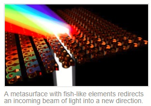
Surfaces that efficiently redirect the propagation of light have been developed by A*STAR researchers. Ramón Paniagua-Domínguez, working with colleagues from the A*STAR Data Storage Institute and Nanyang Technological University, has invented compact and light-weight optical components that could be integrated into portable optoelectronic devices.
Traditional glass optical components alter the propagation of light through reflection and refraction. They tend to be three-dimensional: a lens, for example, requires a curved surface that focuses light to a point. But these bulky elements add weight, to mobile phone cameras for example.
A flatter alternative is found in metasurfaces, which consist of an array of structures, each smaller than the wavelength of light, engineered to modify the characteristics of incident light. As an optical beam hits this surface, it scatters off the subwavelength elements, forming an output beam with chosen properties. This can, for example, be used to bend the incoming beam into a new direction. However, the efficiency with which the light is redistributed into the correct direction decreases sharply for increasing angles, making bending light at very large angles difficult.
Paniagua-Domínguez and the team achieve efficient optical channeling at any desired angle using a metasurface comprising an array of asymmetric nanoantennas. Just like normal antennas, they alter the scattering directivity patterns by suppressing or enhancing emission at different angles. “Our new approach goes beyond the standard design, which is to use phase mapping,” explains Paniagua-Domínguez. “We foresee that these metasurfaces may out-perform traditional bulk optics not only in terms of efficiency, but also functionality.”
The researchers demonstrated this concept experimentally by etching their nanoantenna array design into a thin film of titanium dioxide on a glass substrate. One design they investigated had a structure that loosely resembled a fish, with a ring surrounding one vertex of a triangle. The dimensions of the fish were all below 300 nanometers, much smaller that the wavelength of the incident light. With this novel approach they were able to bend more than 50 per cent of the energy of an incoming beam of green light at an angle of up to 73 degrees. Moreover, and contrary to previous approaches, this structure demonstrated broadband operation, effectively bending light across wavelengths in the green and blue parts of the spectrum.
“Based on this concept, we are now working towards a flat lens with an extremely large numerical aperture,” says Paniagua-Domínguez. “That is, a lens that can focus light into a very small spot or resolve very small objects or features.”
Share on:


Testimonial
"In a year when every marketing dollar mattered, I chose to keep I-Connect007 in our 2025 plan. Their commitment to high-quality, insightful content aligns with Koh Young’s values and helps readers navigate a changing industry. "
Brent Fischthal - Koh YoungSuggested Items
ASM Technologies Limited signs MoU with the Guidance, Government of Tamilnadu to Expand Design-Led Manufacturing capabilities for ESDM
09/15/2025 | ASM TechnologiesASM Technologies Limited, a pioneer in Design- Led Manufacturing in the semiconductor and automotive industries, announced signing of Memorandum of Understanding (MoU) with the Guidance, Government of Tamilnadu whereby it will invest Rs. 250 crores in the state to expand its ESDM related Design-Led Manufacturing and precision engineering capacity. ASM Technologies will acquire 5 acres of land from the Government of Tamilnadu to set up a state-of-the-art design facility in Tamil Nadu's growing technology manufacturing ecosystem, providing a strong strategic advantage and long-term benefits for ASM.
Variosystems Strengthens North American Presence with Southlake Relaunch 2025
09/15/2025 | VariosystemsVariosystems celebrated the relaunch of its U.S. facility in Southlake, Texas. After months of redesign and reorganization, the opening marked more than just the return to a modernized production site—it was a moment to reconnect with our teams, partners, and the local community.
Deca, Silicon Storage Technology Announce Strategic Collaboration to Enable NVM Chiplet Solutions
09/11/2025 | Microchip Technology Inc.As traditional monolithic chip designs grow in complexity and increase in cost, the interest and adoption of chiplet technology in the semiconductor industry also increases.
I-Connect007 Launches New Podcast Series on Ultra High Density Interconnect (UHDI)
09/10/2025 | I-Connect007I-Connect007 is excited to announce the debut of its latest podcast series, which shines a spotlight on one of the most important emerging innovations in electronics manufacturing: Ultra-High-Density Interconnect (UHDI). The series kicks off with Episode One, “Ultra HDI: What does it mean to people? Why would they want it?” Host Nolan Johnson is joined by guest expert John Johnson, Director of Quality and Advanced Technology at American Standard Circuits (ASC).
Global Citizenship: Together for a Perfect PCB Solution
09/10/2025 | Tom Yang -- Column: Global CitizenshipIf there’s one thing we’ve learned in the past few decades of electronics evolution, it’s that no region has a monopoly on excellence. Whether it’s materials science breakthroughs in Europe, manufacturing efficiencies in China, or design innovations in Silicon Valley, the PCB industry thrives on collaboration.