


 Trouble in Your Tank: Implementing Direct Metallization in Advanced Substrate Packaging
 It’s Only Common Sense: Storytelling That Sells—Stop Pitching, Start Painting Pictures
 The Right Approach: Get Ready for ISO 9001 Version 6


A Marriage of Light-Manipulation Technologies
February 28, 2018 | Argonne National LaboratoryEstimated reading time: 3 minutes
Researchers have, for the first time, integrated two technologies widely used in applications such as optical communications, bio-imaging and Light Detection and Ranging (LIDAR) systems that scan the surroundings of self-driving cars and trucks.
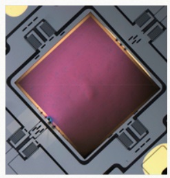
Image caption: This image gives a close-up view of a metasurface-based flat lens (square piece) integrated onto a MEMS scanner. Integration of MEMS devices with metalenses will help manipulate light in sensors by combining the strengths of high-speed dynamic control and precise spatial manipulation of wave fronts. This image was taken with an optical microscope at Argonne’s Center for Nanoscale Materials.
In the collaborative effort between the U.S. Department of Energy’s (DOE) Argonne National Laboratory and Harvard University, researchers successfully crafted a metasurface-based lens atop a Micro-Electro-Mechanical System (MEMS) platform. The result is a new infrared light-focusing system that combines the best features of both technologies while reducing the size of the optical system.
Metasurfaces can be structured at the nanoscale to work like lenses. These metalenses were pioneered by Federico Capasso, Harvard’s Robert L. Wallace Professor of Applied Physics, and his group at the Harvard John A. Paulson School of Engineering and Applied Sciences (SEAS). The lenses are rapidly finding applications because they are much thinner and less bulky than existing lenses, and can be made with the same technology used to fabricate computer chips. The MEMSs, meanwhile, are small mechanical devices that consist of tiny, movable mirrors.
“These devices are key today for many technologies. They have become technologically pervasive and have been adopted for everything from activating automobile air bags to the global positioning systems of smart phones,” said Daniel Lopez, Nanofabrication and Devices Group Leader at Argonne’s Center for Nanoscale Materials, a DOE Office of Science User Facility.
Lopez, Capasso and four co-authors describe how they fabricated and tested their new device in an article in APL Photonics, titled “Dynamic metasurface lens based on MEMS technology.” The device measures 900 microns in diameter and 10 microns in thickness (a human hair is approximately 50 microns thick).
The collaboration’s ongoing work to further develop novel applications for the two technologies is conducted at Argonne’s Center for Nanoscale Materials, SEAS and the Harvard Center for Nanoscale Systems, which is part of the National Nanotechnology Coordinated Infrastructure.
In the technologically merged optical system, MEMS mirrors reflect scanned light, which the metalens then focuses without the need for an additional optical component such as a focusing lens. The challenge that the Argonne/Harvard team overcame was to integrate the two technologies without hurting their performance.
The eventual goal would be to fabricate all components of an optical system — the MEMS, the light source and the metasurface-based optics — with the same technology used to manufacture electronics today.
“Then, in principle, optical systems could be made as thin as credit cards,” Lopez said.
These lens-on-MEMS devices could advance the LIDAR systems used to guide self-driving cars. Current LIDAR systems, which scan for obstacles in their immediate proximity, are, by contrast, several feet in diameter.
“You need specific, big, bulky lenses, and you need mechanical objects to move them around, which is slow and expensive,” said Lopez.
“This first successful integration of metalenses and MEMS, made possible by their highly compatible technologies, will bring high speed and agility to optical systems, as well unprecedented functionalities,” said Capasso.
This work was also supported by the Air Force Office of Scientific Research, the National Science Foundation and the Singapore Agency for Science, Technology and Research’s National Science Scholarship.
About Argonne National Laboratory
Argonne National Laboratory seeks solutions to pressing national problems in science and technology. The nation's first national laboratory, Argonne conducts leading-edge basic and applied scientific research in virtually every scientific discipline. Argonne researchers work closely with researchers from hundreds of companies, universities, and federal, state and municipal agencies to help them solve their specific problems, advance America's scientific leadership and prepare the nation for a better future. With employees from more than 60 nations, Argonne is managed by UChicago Argonne, LLC for the U.S. Department of Energy's Office of Science.
About U.S. Department of Energy's Office of Science
The U.S. Department of Energy's Office of Science is the single largest supporter of basic research in the physical sciences in the United States and is working to address some of the most pressing challenges of our time.
Share on:


Testimonial
"In a year when every marketing dollar mattered, I chose to keep I-Connect007 in our 2025 plan. Their commitment to high-quality, insightful content aligns with Koh Young’s values and helps readers navigate a changing industry. "
Brent Fischthal - Koh YoungSuggested Items
India’s Aerospace and Defence Engineered for Power, Driven by Electronics
09/16/2025 | Gaurab Majumdar, Global Electronics AssociationWith a defence budget of $82.05 billion (2025–26) and a massive $223 billion earmarked for aerospace and defence spending over the next decade, India is rapidly positioning itself as a major player in the global defence and aerospace market.
VIDEOTON EAS's Bulgarian Subsidiary Expands Into Automotive Products
09/15/2025 | VideotonVEAS Bulgaria, engaged in electronics manufacturing, has joined the ranks of VIDEOTON companies authorized to produce automotive products.
Variosystems Strengthens North American Presence with Southlake Relaunch 2025
09/15/2025 | VariosystemsVariosystems celebrated the relaunch of its U.S. facility in Southlake, Texas. After months of redesign and reorganization, the opening marked more than just the return to a modernized production site—it was a moment to reconnect with our teams, partners, and the local community.
Hanwha Aerospace to Collaborate with BAE Systems on Advanced Anti-jamming GPS for Guided Missiles
09/15/2025 | HanwhaHanwha Aerospace has signed a contract with BAE Systems to integrate next-generation, anti-jamming Global Positioning System (GPS) technology into Hanwha Aerospace’s Deep Strike Capability precision-guided weapon system.
EV Group Achieves Breakthrough in Hybrid Bonding Overlay Control for Chiplet Integration
09/12/2025 | EV GroupEV Group (EVG), a leading provider of innovative process solutions and expertise serving leading-edge and future semiconductor designs and chip integration schemes, today unveiled the EVG®40 D2W—the first dedicated die-to-wafer overlay metrology platform to deliver 100 percent die overlay measurement on 300-mm wafers at high precision and speeds needed for production environments. With up to 15X higher throughput than EVG’s industry benchmark EVG®40 NT2 system designed for hybrid wafer bonding metrology, the new EVG40 D2W enables chipmakers to verify die placement accuracy and take rapid corrective action, improving process control and yield in high-volume manufacturing (HVM).