


 Trouble in Your Tank: Implementing Direct Metallization in Advanced Substrate Packaging
 It’s Only Common Sense: Storytelling That Sells—Stop Pitching, Start Painting Pictures
 The Right Approach: Get Ready for ISO 9001 Version 6


Atomic Movies Explain Why Perovskite Solar Cells Are More Efficient
March 2, 2018 | U.S. Department of Energy, Office of ScienceEstimated reading time: 1 minute
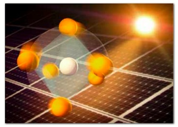
Sunlight causes large changes to the underlying network of atoms that make up perovskites, a promising material for solar cells. Before being hit with light, six iodine atoms rest around a lead atom. Within 10 trillionths of a second after being hit with light, the iodine atoms whirl around each lead atom.
Image caption: Iodine atoms (gold) in perovskites respond to light with unusual rotational motions and distortions around a lead atom (white). These changes could explain the high efficiency of these next-generation solar cell (bottom) materials. (Image: Greg Stewart, SLAC National Accelerator Laboratory)
These first atomic steps distort the structure and result in long-lived changes, similar in size to those observed in melting crystals. Further, the atoms’ motions alter the way electricity moves and may help explain the efficiency of perovskites in solar cells.
In recent years, perovskites have become superstars in the solar cell industry. They are cheap and easy to produce. Despite their popularity, scientists don’t know why perovskites are so efficient. This work shows how atoms in perovskites respond to light and could explain the high efficiency of these next-generation solar cell materials.
Although perovskite solar cell efficiencies have climbed above the 20 percent mark, the fundamental mechanism responsible for these efficiencies is not understood.
To gain insights into the mechanisms, researchers created stop-motion movies of the atoms involved just after the light hits the hybrid perovskites, made from lead, iodine, and methylammonium.
The iodine atoms are arranged in octohedra, eight-sided structures that look like two pyramids joined at their bases. The lead atoms sit inside the octohedra; the methylammonium molecules sit between octohedra. This architecture is common to many of the perovskites investigated for solar cell applications.
At SLAC, researchers hit a perovskite film with two bursts from ultrafast lasers. The technique, called ultrafast electron diffraction, lets them reconstruct the atomic structure. By repeating the experiment with different time delays between the first and second pulse of electrons, the team created a stop-motion movement of the iodine atoms whirling around the lead atoms. That is, a rotationally disordered halide octahedral structure formed in the picoseconds after the light struck.
This work shows the important role of light-induced structural deformations within the lead-iodine lattice. These structural changes could alter the way that charges (electrons and their associated holes) move in hybrid perovskites and provide new information about solar cell efficiencies.
Share on:


Testimonial
"We’re proud to call I-Connect007 a trusted partner. Their innovative approach and industry insight made our podcast collaboration a success by connecting us with the right audience and delivering real results."
Julia McCaffrey - NCAB GroupSuggested Items
Intel Announces Key Leadership Appointments to Accelerate Innovation and Strengthen Execution
09/09/2025 | Intel CorporationIntel Corporation today announced a series of senior leadership appointments that support the company’s strategy to strengthen its core product business, build a trusted foundry, and foster a culture of engineering across the business.
Summit Interconnect Announces Appointment of Leo LaCroix as Chief Operating Officer
09/09/2025 | Summit Interconnect, Inc.Summit Interconnect, a leading North American manufacturer of Printed Circuit Boards (PCBs), today announced that Leo LaCroix has assumed the role of Chief Operating Officer (COO).
Leadership Change at Koh Young Europe
08/14/2025 | Koh YoungAfter 16 years of leading Koh Young Europe as General Manager, we would like to announce that Harald Eppinger will step down from his executive role.
TTM Technologies, Inc. Announces Retirement Plans of its CEO and Proceeds with CEO Successor Search
08/04/2025 | TTM Technologies, Inc.TTM Technologies, Inc., a leading global manufacturer of technology solutions including mission systems, radio frequency (“RF”) components and RF microwave/microelectronic assemblies, quick-turn and technologically advanced printed circuit boards (“PCB”), today announced that Thomas T. Edman, the company’s President and Chief Executive Officer, intends to retire following the appointment of the company’s next President and CEO.
Advancing Electrolytic Copper Plating for AI-driven Package Substrates
08/05/2025 | Dirk Ruess and Mustafa Oezkoek, MKS’ AtotechThe rise of artificial intelligence (AI) applications has become a pivotal force driving growth in the server industry. Its challenging requirements for high-frequency and high-density computing are leading to an increasing demand for development of advanced manufacturing methods of package substrates with finer features, higher hole densities, and denser interconnects. These requirements are essential for modern multilayer board (MLB) designs, which play a critical role in AI hardware. However, these intricate designs introduce considerable manufacturing complexities.