


 Trouble in Your Tank: Implementing Direct Metallization in Advanced Substrate Packaging
 It’s Only Common Sense: Storytelling That Sells—Stop Pitching, Start Painting Pictures
 The Right Approach: Get Ready for ISO 9001 Version 6


Easy Printing of Biosensors Made of Graphene
March 6, 2018 | Fraunhofer-GesellschaftEstimated reading time: 3 minutes
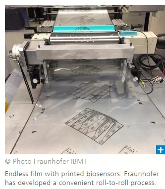
Cell-based biosensors can simulate the effect of various substances, such as drugs, on the human body in the laboratory. Depending on the measuring principle, though, producing them can be expensive. As a result, they are often not used. Cost factors for sensors that perform measurements electrically are the expensive electrode material and complex production. Fraunhofer scientists are now producing biosensors with graphene electrodes cheaply and simply in roll-to-roll printing. A system prototype for mass production already exists.
Cell-based biosensors measure changes in cell cultures via electrical signals. This is done by means of electrodes which are mounted inside the Petri dish or the wells of a so-called well plate. If added viruses destroy a continuous cell layer on the electrodes, for example, the electrical resistance measured between the electrodes is reduced. In this way, the effect of vaccines or drugs (for example) can be tested: the more effective the active ingredient is, the smaller the number of cells that are destroyed by the viruses and the lower the measured resistance change will be. Also toxicity tests, such as on cosmetic products, can function according to the same principle and may replace animal experiments in the future. Another advantage: If biosensors are linked to an evaluation unit, measurements can be continuous and automated.
Conductive, biocompatible, printable
The preparation of the described biosensors is expensive and complex, though: the electrodes are made of a biocompatible and electrically conductive material, such as gold or platinum. The production of microelectrodes requires a complicated lithographic process. The result: The laboratories often do not buy these biosensors because of the high costs, and the examination of the cell cultures continues to be performed manually under a microscope. As an alternative to precious metals, however, graphene can now be used as a material for the electrodes. The advantages of the carbon material: it is electrically conductive, biocompatible and, if in the form of an ink, can be printed on surfaces.
Scientists at the Fraunhofer Institute for Biomedical Engineering IBMT in St. Ingbert in Germany’s Saarland region have made use of such a graphene ink. Together with industry partners in the M-era.Net project BIOGRAPHY, which is funded by the German Federal Ministry of Education and Research (BMBF), they have developed a printing process which makes it possible to produce large numbers of graphene biosensors in a cost-effective roll-to-roll process. "Our system prototype can print about 400 biosensors per minute on a continuous foil," Dr. Thomas Velten, Head of the Biomedical Microsystems Department at IBMT and Project Manager of BIOGRAPHY, says in describing the result of the development work. While the printing equipment and graphene ink are provided by the partners involved, the scientists at the IBMT have taken care of the design of the printing process. "In particular, it is crucial to adjust parameters such as the ink viscosity, printing speed, doctor blade pressure – a doctor blade wipes off excess ink – and well depth of the printing cylinder so that the printed structures correspond to the nominal dimensions," explains Velten. An interdisciplinary team of biologists and engineers from the IBMT have also developed a protein ink, which is printed directly onto the electrodes after the graphene. Velten: "It’s only thanks to the proteins that the cells adhere well enough to the electrode foil". A complicated process: the surface energies of the foil and ink have to be adapted to one another in such a way that the transfer of the ink from the printing cylinder to the foil takes place optimally. Particularly critical is the drying of the printed structures, since the proteins do not tolerate solvents or high temperatures. Only the right mix of ink ingredients and drying method ensures that the ink will dry quickly enough.
After the successful construction of the prototype, the practical tests of the printed biosensors will follow. Project Manager Velten: "We expect to be able to offer the industry a universal technology platform in no later than a year".
Share on:


Testimonial
"The I-Connect007 team is outstanding—kind, responsive, and a true marketing partner. Their design team created fresh, eye-catching ads, and their editorial support polished our content to let our brand shine. Thank you all! "
Sweeney Ng - CEE PCBSuggested Items
Sustainability and Selective Soldering
09/15/2025 | Dr. Samuel J. McMaster, Pillarhouse InternationalSustainability is more than just a buzzword for the electronics industry; it’s a key goal for all manufacturing processes. This is more than a box-ticking exercise or simply doing a small part for environmentally friendly processes. Moving toward sustainable solutions drives innovation and operational efficiency.
Trouble in Your Tank: Implementing Direct Metallization in Advanced Substrate Packaging
09/15/2025 | Michael Carano -- Column: Trouble in Your TankDirect metallization systems based on conductive graphite are gaining popularity throughout the world. The environmental and productivity gains achievable with this process are outstanding. Direct metallization reduces the costs of compliance, waste treatment, and legal issues related to chemical exposure. A graphite-based direct plate system has been devised to address these needs.
EV Group Achieves Breakthrough in Hybrid Bonding Overlay Control for Chiplet Integration
09/12/2025 | EV GroupEV Group (EVG), a leading provider of innovative process solutions and expertise serving leading-edge and future semiconductor designs and chip integration schemes, today unveiled the EVG®40 D2W—the first dedicated die-to-wafer overlay metrology platform to deliver 100 percent die overlay measurement on 300-mm wafers at high precision and speeds needed for production environments. With up to 15X higher throughput than EVG’s industry benchmark EVG®40 NT2 system designed for hybrid wafer bonding metrology, the new EVG40 D2W enables chipmakers to verify die placement accuracy and take rapid corrective action, improving process control and yield in high-volume manufacturing (HVM).
Integrating Uniplate PLBCu6 With the Digital Factory Suite
09/12/2025 | Giovanni Obino and Andreas Schatz, MKS' AtotechPrinted circuit board manufacturing is rapidly changing, driven by miniaturization, stringent reliability requirements, and growing pressure for sustainable production. Meeting these challenges requires more than incremental improvements; it demands a combination of precise equipment and real-time process intelligence. The pairing of Uniplate® PLBCu6 with the Digital Factory Suite (DFS) demonstrates how hardware and software can work together to create more responsive, resource-efficient manufacturing.
Closing the Loop on PCB Etching Waste
09/09/2025 | Shawn Stone, IECAs the PCB industry continues its push toward greener, more cost-efficient operations, Sigma Engineering’s Mecer System offers a comprehensive solution to two of the industry’s most persistent pain points: etchant consumption and rinse water waste. Designed as a modular, fully automated platform, the Mecer System regenerates spent copper etchants—both alkaline and acidic—and simultaneously recycles rinse water, transforming a traditionally linear chemical process into a closed-loop system.