


 Trouble in Your Tank: Implementing Direct Metallization in Advanced Substrate Packaging
 It’s Only Common Sense: Storytelling That Sells—Stop Pitching, Start Painting Pictures
 The Right Approach: Get Ready for ISO 9001 Version 6


New Approach to Measuring Stickiness Could Aid Micro-Device Design
March 8, 2018 | Brown UniversityEstimated reading time: 3 minutes
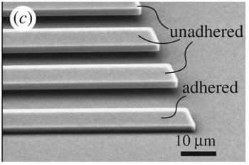
Brown University engineers have devised a new method of measuring the stickiness of micro-scale surfaces. The technique, described in Proceedings of the Royal Society A, could be useful in designing and building micro-electro-mechanical systems (MEMS), devices with microscopic moving parts.
At the scale of bridges or buildings, the most important force that engineered structures need to deal with is gravity. But at the scale of MEMS — devices like the tiny accelerometers used in smartphones and Fitbits — the relative importance of gravity decreases, and adhesive forces become more important.
“The main thing that matters at the microscale is what sticks to what,” said Haneesh Kesari, an assistant professor in Brown’s School of Engineering and coauthor of the new research. “If you have parts of your device sticking together that shouldn’t be, it’s not going to work. So in order to design MEMS devices, it helps to have a good way of measuring adhesion in the materials we use.”
That’s what Kesari and two Brown graduate students, Wenqiang Fang and Joyce Mok, looked to accomplish with this new research. Specifically, they wanted to measure a quantity known as “work of adhesion,” which roughly translates into the amount of energy required to separate a unit area of two adhered surfaces.
The key theoretical insight developed in the new study is that thermal vibrations of a microbeam can be used to calculate work of adhesion. That insight suggests a method in which a slightly modified atomic force microscopy (AFM) system can be used to probe adhesive properties.
Standard AFM works a bit like a record player. A cantilever with a sharp needle moves across a target material. A laser shown on the cantilever measures the tiny undulations it makes as it moves along the material’s contours. Those undulations can then be used to map out the material’s surface properties.
Adapting the method to measure adhesion would require simply removing the metal tip from the cantilever, leaving a flat microbeam. That beam can then be lowered onto a target material, where it will adhere. When the cantilever is raised slightly, some portion of the beam will become unstuck, while the rest remains stuck. The unstuck portion of the beam will vibrate ever so slightly. The authors found a way to use the extent of that vibration, which can be measured by an AFM laser, to calculate the length of the unstuck portion, which can in turn be used to calculate the target material’s work of adhesion.
Fang says the technique could be useful in assessing new material coatings or surface textures aimed at alleviating the failure of MEMS devices through sticking.
“Once you have a robust technique for measuring the material’s work of adhesion, then you have a systematic way of evaluating these methods to get the level of adhesion needed for a particular application,” Fang said. “The main advantage to this method is that you don’t need to change a standard AFM setup very much in order to do this.”
The approach is also much simpler than other techniques, according to Mok.
“Previous methods based on interferometry are labor intensive and may require many data points to be taken,” she said. “Our theoretical framework would give a value for the work of adhesion from a single measurement.”
Having demonstrated the technique numerically, Kesari says the next step is to build the system and start collecting some experimental data. He’s hopeful that such a system will aid in pushing the MEMS field forward.
“We have MEMS accelerometers and gyroscopes, but I don’t think the field has quite lived up to its promise yet,” Kesari said. “Part of the reason for that is that people haven’t completely understood adhesion at the small scale. We think that a more robust way of measuring adhesion is the first step towards gaining such an understanding.”
The research was supported by the National Science Foundation (Grant 1562656) and a Brown Graduate School Presidential Fellowship to Joyce Mok.
Share on:


Testimonial
"The I-Connect007 team is outstanding—kind, responsive, and a true marketing partner. Their design team created fresh, eye-catching ads, and their editorial support polished our content to let our brand shine. Thank you all! "
Sweeney Ng - CEE PCBSuggested Items
I-Connect007 Launches Advanced Electronics Packaging Digest
09/15/2025 | I-Connect007I-Connect007 is pleased to announce the launch of Advanced Electronics Packaging Digest (AEPD), a new monthly digital newsletter dedicated to one of the most critical and rapidly evolving areas of electronics manufacturing: advanced packaging at the interconnect level.
Panasonic Industry will Double the Production Capacity of MEGTRON Multi-layer Circuit Board Materials Over the Next Five Years
09/15/2025 | Panasonic Industry Co., Ltd.Panasonic Industry Co., Ltd., a Panasonic Group company, announced plans for a major expansion of its global production capacity for MEGTRON multi-layer circuit board materials today. The company plans to double its production over the next five years to meet growing demand in the AI server and ICT infrastructure markets.
Trouble in Your Tank: Implementing Direct Metallization in Advanced Substrate Packaging
09/15/2025 | Michael Carano -- Column: Trouble in Your TankDirect metallization systems based on conductive graphite are gaining popularity throughout the world. The environmental and productivity gains achievable with this process are outstanding. Direct metallization reduces the costs of compliance, waste treatment, and legal issues related to chemical exposure. A graphite-based direct plate system has been devised to address these needs.
Fresh PCB Concepts: Designing for Success at the Rigid-flex Transition Area
08/28/2025 | Team NCAB -- Column: Fresh PCB ConceptsRigid-flex PCBs come in all shapes and sizes. Manufacturers typically use fire-retardant, grade 4 (FR-4) materials in the rigid section and flexible polyimide materials in the flex region. Because of the small size, some rigid-flex PCBs, like those for hearing aid devices, are among the most challenging to manufacture. However, regardless of its size, we should not neglect the transition area between the rigid and flexible material.
Global Sourcing Spotlight: How to Evaluate Supplier Capabilities Worldwide
08/20/2025 | Bob Duke -- Column: Global Sourcing SpotlightIn global sourcing, the difference between a competitive edge and a catastrophic disruption often comes down to how well you vet your suppliers. Sourcing advanced PCBs, precision components, or materials for complex assemblies demands diligence, skepticism, and more than a little time on airplanes. Here’s how to do your due diligence when evaluating international suppliers and why cutting corners can cost you more than money.