


 Trouble in Your Tank: Implementing Direct Metallization in Advanced Substrate Packaging
 It’s Only Common Sense: Storytelling That Sells—Stop Pitching, Start Painting Pictures
 The Right Approach: Get Ready for ISO 9001 Version 6


Scaling Silicon Quantum Photonics Technology
March 9, 2018 | ICFOEstimated reading time: 2 minutes
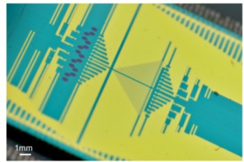
Integrated Quantum Photonics allows the routing and control of single particles of light with intrinsically high stability and precision, however to date it has been limited to small-scale demonstrations in which only a small number of components are integrated on a chip. It is thus in high demand to scale up the integrated photonic circuits and increase the complexity and computational power of modern quantum information processing technologies that would enable many revolutionary applications.
An international team of researchers led by scientists from the Univ. of Bristol’s Quantum Engineering Technology Labs has demonstrated the first ever large-scale integrated quantum photonic circuit, which can generate, control and analyze high-dimensional entanglement with unprecedented high precision and generality. The quantum chip was realised using a scalable silicon photonics technology, similar to today’s electronic circuits, which would provide a path to manufacture massive components for the realization of an optical quantum computer. The work, in collaboration with Peking Uni., Technical Uni. of Denmark (DTU), ICFO – The Institute of Photonic Sciences, Max Planck Institute of Quantum Optics (MPQ), Polish Academy of Sciences (PAS) and Univ. of Copenhagen, has been published recently in the journal Science.
Coherently and precisely controlling large quantum devices and complex multidimensional entanglement systems has been a challenging task owing to the complex interactions of correlated particles in large quantum systems. Significant progress towards large-scale quantum systems has been recently reported in a variety of platforms including photons, superconductors, and ions, among others. In particular, photonics allows a system to naturally encode and process multidimensional qubit states within a photon’s different degrees of freedom. In this work, a programmable bipartite path-encoded multidimensional entangled system with dimension up to 15×15 is demonstrated, where each photon exists over 15 optical paths at the same time and the two photons are entangled with each other there. This multidimensional entanglement system is achieved by scaling up the silicon-photonics quantum circuits via a single chip integration of 550 optical components including 16 identical photon-pair sources, 93 optical phase-shifters, 122 beam-splitters, among other optical elements.
Lead author, Dr Jianwei Wang, said: “It is the maturity of today’s silicon-photonics that allows us to scale up the technology and reach a large-scale integration of quantum circuits. This is the most beautiful thing of quantum photonics on silicon. As a result, our quantum chip allows us to, for the first time, reach the unprecedented high precision and universality of controlling multidimensional entanglement, a key factor in many quantum information tasks of computing and communication.”
ICFO researchers Alexia Salavrakos and Antonio Acín say that "distributing and detecting quantum correlations in a controlled manner is an enabling step to design more robust and secure quantum communication technologies".
Professor Mark Thompson, leader of the Bristol team, has emphasized that "the photonic circuits on silicon, the same material used in our electronic circuits, allow the processing of information carried by a single particle of light. This silicon quantum photonics technologies are allowing us to scale up quantum devices and systems in an incredibly rapid speed, and in the near future it will reach an integration of tens of thousands of elements on a single chip that can promise numerous quantum applications.”
Share on:


Testimonial
"Our marketing partnership with I-Connect007 is already delivering. Just a day after our press release went live, we received a direct inquiry about our updated products!"
Rachael Temple - AlltematedSuggested Items
Electra’s ElectraJet EMJ110 Inkjet Soldermask Now in Black & Blue at Sunrise Electronics
09/08/2025 | Electra Polymers LtdFollowing the successful deployment of Electra’s Green EMJ110 Inkjet Soldermask on KLA’s Orbotech Neos™ platform at Sunrise Electronics in Elk Grove Village, Illinois, production has now moved beyond green.
Magnachip Semiconductor Announces YJ Kim to Step Down as CEO; Current Board Chairman Camillo Martino Appointed Interim CEO
08/14/2025 | PR NewswireMagnachip Semiconductor Corporation today announced that YJ Kim has agreed to step down as CEO and as a member of the Board of Directors, effective immediately. Camillo Martino, Chairman of the Board of Directors, has also been appointed Interim Chief Executive Officer, effective immediately.
Bell to Build X-Plane for Phase 2 of DARPA Speed and Runway Independent Technologies (SPRINT) X-Plane Program
07/09/2025 | Bell Textron Inc.Bell Textron Inc., a Textron Inc. company, has been down-selected for Phase 2 of Defense Advanced Research Projects Agency (DARPA) Speed and Runway Independent Technologies (SPRINT) X-Plane program with the objective to complete design, construction, ground testing and certification of an X-plane demonstrator.
Nolan’s Notes: Moving Forward With Confidence
06/03/2025 | Nolan Johnson -- Column: Nolan's NotesWe’re currently enjoying a revitalized and dynamic EMS provider market with significant growth potential. Since December 2024, the book-to-bill has been extremely strong and growing. Starting with a ratio of 1.24 in December, book-to-bill has continued to accelerate to a 1.41 in April. Yet, there is a global economic restructuring taking place. To say that the back-and-forth with tariffs and trade deals makes for an uncertain market is an understatement. While we may be in a 90-day tariff pause among leading economic nations, the deadline is quickly approaching and that leaves many of you feeling unsettled about what to expect.
Mycronic High Flex Changes Division Name to PCB Assembly Solutions
05/20/2025 | MycronicMycronic AB, the leading Sweden-based electronics assembly solutions provider, announced that its division formerly known as High Flex will now operate under the name PCB Assembly Solutions.