


 Trouble in Your Tank: Implementing Direct Metallization in Advanced Substrate Packaging
 It’s Only Common Sense: Storytelling That Sells—Stop Pitching, Start Painting Pictures
 The Right Approach: Get Ready for ISO 9001 Version 6


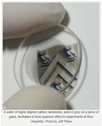
Plasmons Triggered in Nanotube Quantum Wells
March 19, 2018 | Rice UniversityEstimated reading time: 4 minutes
A novel quantum effect observed in a carbon nanotube film could lead to the development of unique lasers and other optoelectronic devices, according to scientists at Rice University and Tokyo Metropolitan University.
The Rice-Tokyo team reported an advance in the ability to manipulate light at the quantum scale by using single-walled carbon nanotubes as plasmonic quantum confinement fields.
The phenomenon found in the Rice lab of physicist Junichiro Kono could be key to developing optoelectronic devices like nanoscale, near-infrared lasers that emit continuous beams at wavelengths too short to be produced by current technology.
The project came together in the wake of the Kono group’s discovery of a way to achieve very tight alignment of carbon nanotubes in wafer-sized films. These films allowed for experiments that were far too difficult to carry out on single or tangled aggregates of nanotubes and caught the attention of Tokyo Metropolitan physicist Kazuhiro Yanagi, who studies condensed matter physics in nano materials.
“He brought the gating technique (which controls the density of electrons in the nanotube film), and we provided the alignment technique,” Kono said. “For the first time we were able to make a large-area film of aligned nanotubes with a gate that allows us to inject and take out a large density of free electrons.”
“The gating technique is very interesting, but the nanotubes were randomly oriented in the films I had used,” Yanagi said. “That situation was very frustrating because I could not get precise knowledge of the one-dimensional characteristics of nanotubes in such films, which is most important. The films that can only be provided by the Kono group are amazing because they allowed us to tackle this subject.”
Their combined technologies let them pump electrons into nanotubes that are little more than a nanometer wide and then excite them with polarized light. The width of the nanotubes trapped the electrons in quantum wells, in which the energy of atoms and subatomic particles is “confined” to certain states, or subbands.
Light then prompted them to oscillate very quickly between the walls. With enough electrons, Kono said, they began to act as plasmons.
“Plasmons are collective charge oscillations in a confined structure,” he said. “If you have a plate, a film, a ribbon, a particle or a sphere and you perturb the system (usually with a light beam), these free carriers move collectively with a characteristic frequency.” The effect is determined by the number of electrons and the size and shape of the object.
Because the nanotubes in the Rice experiments were so thin, the energy between the quantized subbands was comparable to the plasmon energy, Kono said. “This is the quantum regime for plasmons, where the intersubband transition is called the intersubband plasmon. People have studied this in artificial semiconductor quantum wells in the very far-infrared wavelength range, but this is the first time it has been observed in a naturally occurring low-dimensional material and at such a short wavelength.”
Detecting a very complicated gate voltage dependence in the plasmonic response was a surprise, as was its appearance in both metallic and semiconducting single-walled nanotubes. “By examining the basic theory of light-nanotube interactions, we were able to derive a formula for the resonance energy,” Kono said. “To our surprise, the formula was very simple. Only the diameter of the nanotube matters.”
The researchers believe the phenomenon could lead to advanced devices for communications, spectroscopy and imaging, as well as highly tunable near-infrared quantum cascade lasers.
While traditional semiconductor lasers depend on the width of the lasing material’s bandgap, quantum cascade lasers do not, said Weilu Gao, a co-author on the study and a postdoctoral researcher in Kono’s group that is spearheading device development using aligned nanotubes. “The wavelength is independent of the gap,” he said. “Our laser would be in this category. Just by changing the diameter of the nanotube, we should be able to tune the plasma resonance energy without worrying about the bandgap.”
Kono also expects the gated and aligned nanotube films will give physicists the opportunity to study Luttinger liquids, theoretical collections of interacting electrons in one-dimensional conductors.
“One-dimensional metals are predicted to be very different from 2-D and 3-D,” Kono said. “Carbon nanotubes are some of the best candidates for observing Luttinger liquid behaviors. It’s difficult to study a single tube, but we have a macroscopic one-dimensional system. By doping or gating, we can tune the Fermi energy. We can even convert a 1-D semiconductor into a 1-D metal. So this is an ideal system to study this kind of physics.”
Yanagi, a professor of condensed matter physics at Tokyo Metropolitan University, is lead author of the paper. Co-authors are graduate student Ryotaro Okada, graduate student Yota Ichinose and Yohei Yomogida, an assistant professor of condensed matter physics, all at Tokyo Metropolitan, and graduate student Fumiya Katsutani at Rice. Kono is a professor of electrical and computer engineering, of physics and astronomy, and of materials science and nanoengineering.
The research was supported by Japan Society for the Promotion of Science Grant-in-Aid for Scientific Research (KAKENHI) grants, a Japan Science and Technology Core Research of Evolutional Science and Technology grant, the Yamada Science Foundation and the Basic Energy Sciences program of the U.S. Department of Energy, the National Science Foundation and the Robert A. Welch Foundation.
Share on:


Testimonial
"We’re proud to call I-Connect007 a trusted partner. Their innovative approach and industry insight made our podcast collaboration a success by connecting us with the right audience and delivering real results."
Julia McCaffrey - NCAB GroupSuggested Items
MEMS & Imaging Sensors Summit to Spotlight Sensing Revolution for Europe’s Leadership
09/11/2025 | SEMIIndustry experts will gather November 19-20 at the SEMI MEMS & Imaging Sensors Summit 2025 to explore the latest breakthroughs in AI-driven MEMS and imaging optimization, AR/VR technologies, and advanced sensor solutions for critical defence applications.
Direct Imaging System Market Size to Hit $4.30B by 2032, Driven by Increasing Demand for High-Precision PCB Manufacturing
09/11/2025 | Globe NewswireAccording to the SNS Insider, “The Direct Imaging System Market size was valued at $2.21 Billion in 2024 and is projected to reach $4.30 Billion by 2032, growing at a CAGR of 8.68% during 2025-2032.”
I-Connect007’s Editor’s Choice: Five Must-Reads for the Week
07/04/2025 | Marcy LaRont, I-Connect007For our industry, we have seen several bullish market announcements over the past few weeks, including one this week by IDC on the massive growth in the global server market. We’re also closely watching global trade and nearshoring. One good example of successful nearshoring is Rehm Thermal Systems, which celebrates its 10th anniversary in Mexico and the official opening of its new building in Guadalajara.
Driving Innovation: Direct Imaging vs. Conventional Exposure
07/01/2025 | Simon Khesin -- Column: Driving InnovationMy first camera used Kodak film. I even experimented with developing photos in the bathroom, though I usually dropped the film off at a Kodak center and received the prints two weeks later, only to discover that some images were out of focus or poorly framed. Today, every smartphone contains a high-quality camera capable of producing stunning images instantly.
United Electronics Corporation Advances Manufacturing Capabilities with Schmoll MDI-ST Imaging Equipment
06/24/2025 | United Electronics CorporationUnited Electronics Corporation has successfully installed the advanced Schmoll MDI-ST (XL) imaging equipment at their advanced printed circuit board facility. This significant technology investment represents a continued commitment to delivering superior products and maintaining their position as an industry leader in precision PCB manufacturing.