


 Trouble in Your Tank: Implementing Direct Metallization in Advanced Substrate Packaging
 It’s Only Common Sense: Storytelling That Sells—Stop Pitching, Start Painting Pictures
 The Right Approach: Get Ready for ISO 9001 Version 6


Sniffing Out the Foundational Science of Sensors
March 23, 2018 | U.S. Department of EnergyEstimated reading time: 9 minutes
The human nose can distinguish among a trillion different combinations of smells. Even so, there are plenty of gases that our noses can't detect at the level of sensitivity we need. That's where gaseous sensors come in. While some of the first sensors were animals – like canaries in coal mines – we've since replaced them with technologies that can detect miniscule amounts of chemicals in the air.
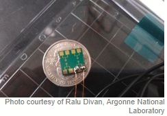
Image caption: This sensor can detect methane at much lower concentrations than current ones. It relies on nanotechnology developed at the Center for Nanoscale Materials, an Office of Science user facility.
Just like our own noses, gaseous sensors are essential for safety and comfort. In factories, gaseous sensors can alert managers to chemical leaks or processes running incorrectly. Outside, they measure pollutants, helping cities monitor air quality. In homes, they keep family members safe. Building managers use measurements from humidity and temperature sensors to maximize energy efficiency.
These sensors wouldn't exist without a fundamental understanding of chemistry and physics. This basic knowledge helps scientists understand how and why sensing materials interact with gaseous chemicals. Many cutting-edge materials have promise for use in sensors, if only scientists can learn how to better produce and control them.
"Sensors are where materials research meets environmental detection," said Pete Beckman, a researcher at Department of Energy's Argonne National Laboratory (ANL).
To set the groundwork for innovation, the DOE Office of Science funds projects and user facilities that support sensors research.
Creating the Materials for Sensing
Like noses, sensors rely on a combination of components to detect and make sense of gases or chemicals in the air. In humans, molecules float up into your nose and bind to special neurons. Neurons then pass the message up to the brain. In sensors, the material inside the sensor acts as a neuron. When that material interacts with a chemical in the air, it may emit light, change its ability to conduct electricity, or shift shape. The materials and electronics around the sensing material communicate that message to the sensor's "brain," whether that brain is a computer or a warning signal like a siren.
Developing sensors' nervous systems and brains is a job for applied science. Fundamental research like the work at the Office of Science's laboratories sets the foundation for that applied science. In particular, this research is expanding scientists' understanding of the materials themselves and how to produce them.
Three types of cutting-edge materials offer huge potential for use in sensors: nanoparticles, two-dimensional (2D) materials, and metal-organic frameworks (MOFs). Nanoparticles are miniscule particles that are bigger than atoms, but act fundamentally differently from larger particles of the same substance. 2D materials, like graphene, form sheets only a single atom thick. MOFs are compounds made of metal ions linked together by carbon-based connectors.
All of these materials have humongous surface areas compared to their overall sizes. Because lots of gas molecules can interact with their surfaces, they can be sensitive to tiny amounts of chemicals. In addition, scientists can craft all of these materials into a variety of structures. That customization could allow researchers to create specialty materials to detect a particular chemical.
Zinc Sulfide Nanoparticles
The key to building a better sensor may lie in making its sensing material out of nanoparticles. Unfortunately, it's challenging to manufacture some of the most promising of those nanoparticles. Sensors for hydrogen and other gases already use the material zinc sulfide. Producing zinc sulfide in nanoparticle form could make it cheaper and more effective. But the current process for producing zinc sulfide nanoparticles involves very high temperatures, pressures, and toxic chemicals.
Scientists at DOE's Oak Ridge National Laboratory (ORNL) investigated a cheaper, more efficient nanoparticle production process. Researchers supported by both DOE's Advanced Manufacturing Office and Office of Science found that microbes may offer an alternative path forwardExternal link.
Not just any bacteria will do. Scientists used Thermoanaerobacter, a bacteria that normally lives in extremely hot places with no oxygen. After adding a cheap sugar and chemicals that included zinc and sulfur, the bacteria produced about three-quarters of a pound of zinc sulfide nanoparticles. The process was 90 percent cheaper than current methods.
Page 1 of 3
Share on:


Testimonial
"Advertising in PCB007 Magazine has been a great way to showcase our bare board testers to the right audience. The I-Connect007 team makes the process smooth and professional. We’re proud to be featured in such a trusted publication."
Klaus Koziol - atgSuggested Items
Trouble in Your Tank: Implementing Direct Metallization in Advanced Substrate Packaging
09/15/2025 | Michael Carano -- Column: Trouble in Your TankDirect metallization systems based on conductive graphite are gaining popularity throughout the world. The environmental and productivity gains achievable with this process are outstanding. Direct metallization reduces the costs of compliance, waste treatment, and legal issues related to chemical exposure. A graphite-based direct plate system has been devised to address these needs.
Closing the Loop on PCB Etching Waste
09/09/2025 | Shawn Stone, IECAs the PCB industry continues its push toward greener, more cost-efficient operations, Sigma Engineering’s Mecer System offers a comprehensive solution to two of the industry’s most persistent pain points: etchant consumption and rinse water waste. Designed as a modular, fully automated platform, the Mecer System regenerates spent copper etchants—both alkaline and acidic—and simultaneously recycles rinse water, transforming a traditionally linear chemical process into a closed-loop system.
Driving Innovation: Depth Routing Processes—Achieving Unparalleled Precision in Complex PCBs
09/08/2025 | Kurt Palmer -- Column: Driving InnovationIn PCB manufacturing, the demand for increasingly complex and miniaturized designs continually pushes the boundaries of traditional fabrication methods, including depth routing. Success in these applications demands not only on robust machinery but also sophisticated control functions. PCB manufacturers rely on advanced machine features and process methodologies to meet their precise depth routing goals. Here, I’ll explore some crucial functions that empower manufacturers to master complex depth routing challenges.
Trouble in Your Tank: Minimizing Small-via Defects for High-reliability PCBs
08/27/2025 | Michael Carano -- Column: Trouble in Your TankTo quote the comedian Stephen Wright, “If at first you don’t succeed, then skydiving is not for you.” That can be the battle cry when you find that only small-diameter vias are exhibiting voids. Why are small holes more prone to voids than larger vias when processed through electroless copper? There are several reasons.
The Government Circuit: Navigating New Trade Headwinds and New Partnerships
08/25/2025 | Chris Mitchell -- Column: The Government CircuitAs global trade winds continue to howl, the electronics manufacturing industry finds itself at a critical juncture. After months of warnings, the U.S. Government has implemented a broad array of tariff increases, with fresh duties hitting copper-based products, semiconductors, and imports from many nations. On the positive side, tentative trade agreements with Europe, China, Japan, and other nations are providing at least some clarity and counterbalance.