


 Trouble in Your Tank: Implementing Direct Metallization in Advanced Substrate Packaging
 It’s Only Common Sense: Storytelling That Sells—Stop Pitching, Start Painting Pictures
 The Right Approach: Get Ready for ISO 9001 Version 6


Femtosecond Laser Fabrication: Realizing Dynamics Control of Electrons
March 27, 2018 | Changchun Institute of Optics, Fine Mechanics and PhysicsEstimated reading time: 1 minute
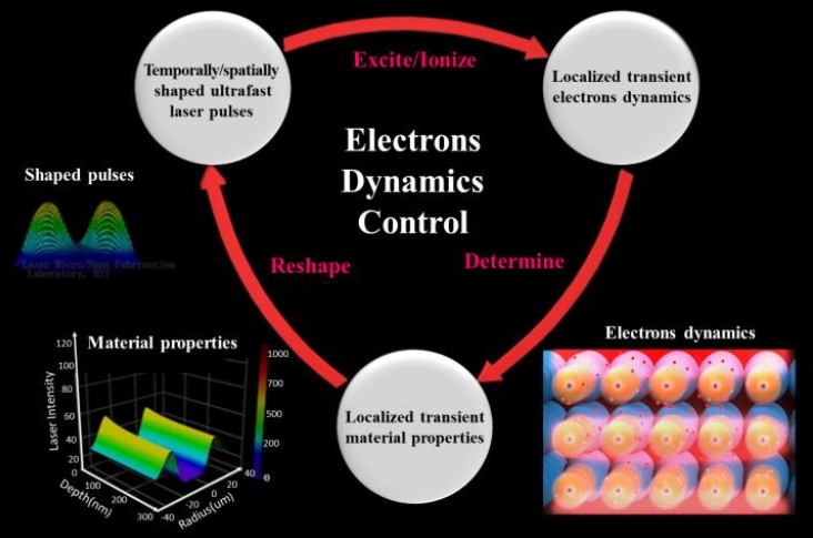
Femtosecond lasers are capable of processing any solid material with high quality and high precision using their ultrafast and ultra-intense characteristics. With the continuous development of laser technology, ultrafast laser manufacturing would hopefully become one of the primary methods employed in high-end manufacturing in the future.
Recently, researchers realized a new method termed electrons dynamics control for ultrafast laser micro/nano fabrication. For the first time, the localized transient electrons dynamics in laser fabrication can be actively controlled to manipulate material properties, which greatly enhances the efficiency, quality, uniformity, and precision of laser fabrication.
This research is conducted by the group of Professor Lan Jiang from Beijing Institute of Technology, in cooperation with Professor Tian-Hong Cui from Minnesota University, Twin City, and Professor Yongfeng Lu from Nebraska University, Lincoln. Their research results were recently reviewed in Light: Science and Applications.
Over the past decade, the research group has devoted their efforts to studying novel methods of manufacturing based on electrons dynamics control. They used the temporally/spatially shaped ultrafast laser to control the localized transient electron dynamics (e.g., density, temperature, and distribution); furthermore, they modified the localized transient material properties and adjusted material phase change; eventually, they implemented the novel fabrication method.
They established a multiscale model of ultrafast laser materials interactions and predicted that the temporally/spatially shaped ultrafast pulses can control the laser material interaction processes. Furthermore, on the basis of the theoretical predictions, they experimentally verified the validity of the electrons dynamics control method. In addition, they proposed and implemented a multiscale measurement system for observing femtosecond laser ablation dynamics from femtosecond scale to second scale, which provided experimental evidences for the proposed mechanism.
Using this method, they greatly improved fabrication efficiency, quality, repeatability, and precision, as well as extended the fabrication limits of laser manufacturing. The new method has resolved some critical manufacturing challenges and already been applied to a series of major Chinese national projects.
This novel method has realized the active control of localized transient electrons dynamics in the laser fabrication process for the first time. Furthermore, it has opened the wide exciting possibilities in the control of fabrication on electron level, which may provide revolutionary contributions to high-end manufacturing, material properties manipulation, and chemical reactions control.
Share on:


Testimonial
"We’re proud to call I-Connect007 a trusted partner. Their innovative approach and industry insight made our podcast collaboration a success by connecting us with the right audience and delivering real results."
Julia McCaffrey - NCAB GroupSuggested Items
I-Connect007 Launches Advanced Electronics Packaging Digest
09/15/2025 | I-Connect007I-Connect007 is pleased to announce the launch of Advanced Electronics Packaging Digest (AEPD), a new monthly digital newsletter dedicated to one of the most critical and rapidly evolving areas of electronics manufacturing: advanced packaging at the interconnect level.
ICAPE Group Unveils Exclusive Report on Sustainability in Electronics Manufacturing
09/15/2025 | ICAPE GroupICAPE Group, a global leader in printed circuit boards (PCBs) and custom electronics manufacturing, today announces the launch of its 2025 Industry Outlook & Innovation Report: Sustainability in Electronics Manufacturing. This exclusive report is accompanied by fresh insights from a dedicated Statista survey of 100 electronics manufacturing professionals, commissioned by ICAPE Group.
Panasonic Industry will Double the Production Capacity of MEGTRON Multi-layer Circuit Board Materials Over the Next Five Years
09/15/2025 | Panasonic Industry Co., Ltd.Panasonic Industry Co., Ltd., a Panasonic Group company, announced plans for a major expansion of its global production capacity for MEGTRON multi-layer circuit board materials today. The company plans to double its production over the next five years to meet growing demand in the AI server and ICT infrastructure markets.
Sustainability and Selective Soldering
09/15/2025 | Dr. Samuel J. McMaster, Pillarhouse InternationalSustainability is more than just a buzzword for the electronics industry; it’s a key goal for all manufacturing processes. This is more than a box-ticking exercise or simply doing a small part for environmentally friendly processes. Moving toward sustainable solutions drives innovation and operational efficiency.
ASM Technologies Limited signs MoU with the Guidance, Government of Tamilnadu to Expand Design-Led Manufacturing capabilities for ESDM
09/15/2025 | ASM TechnologiesASM Technologies Limited, a pioneer in Design- Led Manufacturing in the semiconductor and automotive industries, announced signing of Memorandum of Understanding (MoU) with the Guidance, Government of Tamilnadu whereby it will invest Rs. 250 crores in the state to expand its ESDM related Design-Led Manufacturing and precision engineering capacity. ASM Technologies will acquire 5 acres of land from the Government of Tamilnadu to set up a state-of-the-art design facility in Tamil Nadu's growing technology manufacturing ecosystem, providing a strong strategic advantage and long-term benefits for ASM.