


 Trouble in Your Tank: Implementing Direct Metallization in Advanced Substrate Packaging
 It’s Only Common Sense: Storytelling That Sells—Stop Pitching, Start Painting Pictures
 The Right Approach: Get Ready for ISO 9001 Version 6


Self-Assembling, Tunable Interfaces Found in Quantum Materials
March 27, 2018 | Los Alamos National LaboratoryEstimated reading time: 2 minutes
A potential revolution in device engineering could be underway, thanks to the discovery of functional electronic interfaces in quantum materials that can self-assemble spontaneously.
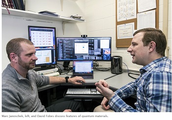
“This illustrates that if we can learn to control and exploit the remarkable properties at the interfaces of quantum materials, this will likely result in a new generation of devices beyond our current imagination,” said Marc Janoschek, a physicist at Los Alamos National Laboratory who, with David Fobes, also of Los Alamos, co-led the international research team making the discovery. Their findings were published today in Nature Physics. “However, because quantum materials are chemically much more complex compared to ‘conventional’ materials such as semiconductors, it remains a challenge to fabricate clean quantum material interfaces.”
Materials with properties characterized by the laws of quantum mechanics rather than classical mechanics often have features such as superconductivity. But extensive research has shown that at interfaces between two materials, the remarkable properties of quantum materials can be strongly enhanced or entirely new functional properties may arise.
An example of the importance of material interfaces would be transistors, whose function is based on physical effects occurring at semiconductor interfaces artificially engineered via techniques such as lithography. Transistors form the foundation for the current generation of electronic devices.
The complexity of quantum materials is often characterized by the competition of various interactions on the quantum level.
“Here we showed that at the same time this complexity also provides a solution,” said Fobes, who carried out his postdoctoral research under the supervision of Janoschek. Fobes and Janoschek led the international team of researchers that combined extensive neutron spectroscopy measurements from Oak Ridge National Laboratory’s (ORNL) Spallation Neutron Source (SNS), National Institute of Standards and Technology’s (NIST) Center for Neutron Research (NCNR), United Kingdom’s Neutron and Muon Source (ISIS), and at the Munich Research Reactor II (FRM II) of the Heinz-Mayer-Leibnitz Zentrum in Germany with detailed theoretical modeling.
“Neutron spectroscopy measurements were crucial to demonstrating that in certain metals, the competition between various interactions may be resolved by the spontaneous formation of a state in which the electronic and magnetic properties alternate periodically,” said Georg Ehlers, the ORNL scientist who performed spectroscopy measurements at SNS.
This periodic arrangement leads to interfaces between alternating material layers that are akin to interfaces in engineered heterostructures. However, the spontaneously self-assembling interfaces identified in this study have major advantages; they are intrinsically clean, and relevant parameters such as the interface thickness can be tuned in-situ via external parameters such as magnetic field or temperature.
The basic ingredients identified by Fobes and the team are common to several classes of quantum materials and suggest that these intrinsic and tunable interfaces may be more frequent. Learning to control the self-assembly of such intrinsic quantum interfaces, in turn, has the potential to revolutionize device design, where devices are not fabricated but spontaneously form via quantum engineering of the underlying atomic-scale interactions. In addition, these devices could be tuned and reconfigured using external parameters, possibly allowing for the design of highly adaptive electronics.
Share on:


Testimonial
"Advertising in PCB007 Magazine has been a great way to showcase our bare board testers to the right audience. The I-Connect007 team makes the process smooth and professional. We’re proud to be featured in such a trusted publication."
Klaus Koziol - atgSuggested Items
I-Connect007 Launches Advanced Electronics Packaging Digest
09/15/2025 | I-Connect007I-Connect007 is pleased to announce the launch of Advanced Electronics Packaging Digest (AEPD), a new monthly digital newsletter dedicated to one of the most critical and rapidly evolving areas of electronics manufacturing: advanced packaging at the interconnect level.
Panasonic Industry will Double the Production Capacity of MEGTRON Multi-layer Circuit Board Materials Over the Next Five Years
09/15/2025 | Panasonic Industry Co., Ltd.Panasonic Industry Co., Ltd., a Panasonic Group company, announced plans for a major expansion of its global production capacity for MEGTRON multi-layer circuit board materials today. The company plans to double its production over the next five years to meet growing demand in the AI server and ICT infrastructure markets.
Trouble in Your Tank: Implementing Direct Metallization in Advanced Substrate Packaging
09/15/2025 | Michael Carano -- Column: Trouble in Your TankDirect metallization systems based on conductive graphite are gaining popularity throughout the world. The environmental and productivity gains achievable with this process are outstanding. Direct metallization reduces the costs of compliance, waste treatment, and legal issues related to chemical exposure. A graphite-based direct plate system has been devised to address these needs.
Fresh PCB Concepts: Designing for Success at the Rigid-flex Transition Area
08/28/2025 | Team NCAB -- Column: Fresh PCB ConceptsRigid-flex PCBs come in all shapes and sizes. Manufacturers typically use fire-retardant, grade 4 (FR-4) materials in the rigid section and flexible polyimide materials in the flex region. Because of the small size, some rigid-flex PCBs, like those for hearing aid devices, are among the most challenging to manufacture. However, regardless of its size, we should not neglect the transition area between the rigid and flexible material.
Global Sourcing Spotlight: How to Evaluate Supplier Capabilities Worldwide
08/20/2025 | Bob Duke -- Column: Global Sourcing SpotlightIn global sourcing, the difference between a competitive edge and a catastrophic disruption often comes down to how well you vet your suppliers. Sourcing advanced PCBs, precision components, or materials for complex assemblies demands diligence, skepticism, and more than a little time on airplanes. Here’s how to do your due diligence when evaluating international suppliers and why cutting corners can cost you more than money.