


 Trouble in Your Tank: Implementing Direct Metallization in Advanced Substrate Packaging
 It’s Only Common Sense: Storytelling That Sells—Stop Pitching, Start Painting Pictures
 The Right Approach: Get Ready for ISO 9001 Version 6


New Microsensor Enables Kidney Dialysis to be Customized
March 30, 2018 | TU EindhovenEstimated reading time: 3 minutes
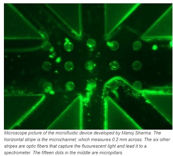
Microscope picture of the microfluidic device developed by Manoj Sharma. The horizontal stripe is the microchannel, which measures 0.2 mm across. The six other stripes are optic fibers that capture the fluourescent light and lead it to a spectrometer. The fifteen dots in the middle are micropillars.
Researchers from TU Eindhoven have developed a microsensor that makes it possible to directly monitor and adjust the composition of kidney dialysis fluid. This is a crucial step towards patient specific dialysis, which will remove a significant proportion of the serious side effects of the use of standard dialysis fluid. On 29 March Manoj Kumar Sharma will be awarded a PhD for his research on this sensor.
Kidney failure makes around two million people worldwide dependent on kidney dialysis to clean their blood. A tube is connected to a blood vessel and the blood is passed along a membrane, with dialysate (dialysis fluid) on the other side. Because the concentration of salts in the blood is higher than in the dialysate, salt passes through the membrane and enters the dialysate. The rate at which this happens depends on the difference in concentration between blood and dialysate. Since the concentration of salts varies widely among different patients, and the concentration in dialysate has the same standard value, the speed is often not ideal. This causes serious side effects, such as heart rhythm disturbance and renal bone disease. It would be better to continuously adjust the concentrations of salts in the dialysate so that they are optimal for the patient. This, however, requires that the concentrations of salts in the dialysate can be monitored live, but there had not been a reliable technique for that to date.
Micropillars
Manoj Kumar Sharma has devised an ingenious solution for this. He developed a micro-system with a centrally positioned microchannel through which dialysate flows. He covered the walls of the microchannel with sensor molecules, which are only fluorescent in the presence of a salt, such as sodium. The more sodium there is in the dialysate, the stronger the fluorescence. To reinforce this effect, he introduced micropillars into the microchannel, resulting in even more surface covered with sensor molecules.
Analysis
A laser light shines on the microchannel, and activates the fluorescence of the sensor molecules. Sharma captures this fluorescence using glass fibers that he connected to the channel in the micro-system. The light passes through the fibers to a spectrometer for analysis. The laser light, which is of a different wavelength, is first filtered out. Then, based on the measured intensity of the fluorescence, the sodium concentrations can be read out.
Pure Measurement
It is important to ensure that the sensor molecules are not disturbed by other salts, so that a pure measurement of the concentration of a specific salt is possible. The ‘microfluidic sensor system’ of approximately 5x2 centimeters built by the Eindhoven researcher is able to measure sodium, the most important salt in the blood, accurately and live. He expects that it will be relatively easy to extend the micro-system with channel sections coated with other ‘photo-induced electron transfer’ (PET) sensor molecules, which are sensitive to the other essential salts, such as potassium and phosphate.
1x1 Centimeter
Sharma thinks that his technique has a very good chance of being used in dialysis machines. The technique is relatively cheap, stable and very accurate. In addition, he expects that the size of his sensor system can be further reduced, to about 1x1 centimeter, facilitating integration into dialysis machines. His technique may also eventually become part of a portable artificial kidney, a solution that will significantly ease the life of kidney patients.
Sharma carried out his research in collaboration with Maastricht UMC + and TNO and with the support of the Dutch Kidney Foundation.
Share on:


Testimonial
"Advertising in PCB007 Magazine has been a great way to showcase our bare board testers to the right audience. The I-Connect007 team makes the process smooth and professional. We’re proud to be featured in such a trusted publication."
Klaus Koziol - atgSuggested Items
I-Connect007 Launches Advanced Electronics Packaging Digest
09/15/2025 | I-Connect007I-Connect007 is pleased to announce the launch of Advanced Electronics Packaging Digest (AEPD), a new monthly digital newsletter dedicated to one of the most critical and rapidly evolving areas of electronics manufacturing: advanced packaging at the interconnect level.
VIDEOTON EAS's Bulgarian Subsidiary Expands Into Automotive Products
09/15/2025 | VideotonVEAS Bulgaria, engaged in electronics manufacturing, has joined the ranks of VIDEOTON companies authorized to produce automotive products.
Variosystems Strengthens North American Presence with Southlake Relaunch 2025
09/15/2025 | VariosystemsVariosystems celebrated the relaunch of its U.S. facility in Southlake, Texas. After months of redesign and reorganization, the opening marked more than just the return to a modernized production site—it was a moment to reconnect with our teams, partners, and the local community.
Hanwha Aerospace to Collaborate with BAE Systems on Advanced Anti-jamming GPS for Guided Missiles
09/15/2025 | HanwhaHanwha Aerospace has signed a contract with BAE Systems to integrate next-generation, anti-jamming Global Positioning System (GPS) technology into Hanwha Aerospace’s Deep Strike Capability precision-guided weapon system.
EV Group Achieves Breakthrough in Hybrid Bonding Overlay Control for Chiplet Integration
09/12/2025 | EV GroupEV Group (EVG), a leading provider of innovative process solutions and expertise serving leading-edge and future semiconductor designs and chip integration schemes, today unveiled the EVG®40 D2W—the first dedicated die-to-wafer overlay metrology platform to deliver 100 percent die overlay measurement on 300-mm wafers at high precision and speeds needed for production environments. With up to 15X higher throughput than EVG’s industry benchmark EVG®40 NT2 system designed for hybrid wafer bonding metrology, the new EVG40 D2W enables chipmakers to verify die placement accuracy and take rapid corrective action, improving process control and yield in high-volume manufacturing (HVM).