


 Trouble in Your Tank: Implementing Direct Metallization in Advanced Substrate Packaging
 It’s Only Common Sense: Storytelling That Sells—Stop Pitching, Start Painting Pictures
 The Right Approach: Get Ready for ISO 9001 Version 6


Stretchable, Twistable Wires for Wearable Electronics
April 3, 2018 | Duke UniversityEstimated reading time: 1 minute
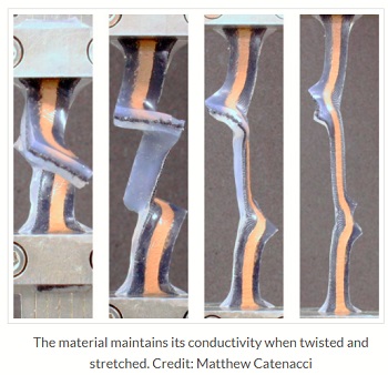
The exercise-tracking power of a Fitbit may soon jump from your wrist and into your clothing.
Researchers are seeking to embed electronics such as fitness trackers and health monitors into our shirts, hats, and shoes. But no one wants stiff copper wires or silicon transistors deforming their clothing or poking into their skin.
Scientists in Benjamin Wiley’s lab at Duke have created new conductive “felt” that can be easily patterned onto fabrics to create flexible wires. The felt, composed of silver-coated copper nanowires and silicon rubber, carries electricity even when bent, stretched and twisted, over and over again.
“We wanted to create wiring that is stretchable on the body,” said Matthew Catenacci, a graduate student in Wiley’s group.
To create a flexible wire, the team first sucks a solution of copper nanowires and water through a stencil, creating a stack of interwoven nanowires in the desired shape. The material is similar to the interwoven fibers that comprise fabric felt, but on a much smaller scale, said Wiley, an associate professor of chemistry at Duke.
“The way I think about the wires are like tiny sticks of uncooked spaghetti,” Wiley said. “The water passes through, and then you end up with this pile of sticks with a high porosity.”
The interwoven nanowires are heated to 300 F to melt the contacts together, and then silicone rubber is added to fill in the gaps between the wires.
To show the pliability of their new material, Catenacci patterned the nanowire felt into a variety of squiggly, snaking patterns. Stretching and twisting the wires up to 300 times did not degrade the conductivity.
“On a larger scale you could take a whole shirt, put it over a vacuum filter, and with a stencil you could create whatever wire pattern you want,” Catenacci said. “After you add the silicone, so you will just have a patch of fabric that is able to stretch.”
Their felt is not the first conductive material that displays the agility of a gymnast. Flexible wires made of silver microflakes also exhibit this unique set of properties. But the new material has the best performance of any other material so far, and at a much lower cost.
“This material retains its conductivity after stretching better than any other material with this high of an initial conductivity. That is what separates it,” Wiley said.
Share on:


Testimonial
"We’re proud to call I-Connect007 a trusted partner. Their innovative approach and industry insight made our podcast collaboration a success by connecting us with the right audience and delivering real results."
Julia McCaffrey - NCAB GroupSuggested Items
Trouble in Your Tank: Implementing Direct Metallization in Advanced Substrate Packaging
09/15/2025 | Michael Carano -- Column: Trouble in Your TankDirect metallization systems based on conductive graphite are gaining popularity throughout the world. The environmental and productivity gains achievable with this process are outstanding. Direct metallization reduces the costs of compliance, waste treatment, and legal issues related to chemical exposure. A graphite-based direct plate system has been devised to address these needs.
Closing the Loop on PCB Etching Waste
09/09/2025 | Shawn Stone, IECAs the PCB industry continues its push toward greener, more cost-efficient operations, Sigma Engineering’s Mecer System offers a comprehensive solution to two of the industry’s most persistent pain points: etchant consumption and rinse water waste. Designed as a modular, fully automated platform, the Mecer System regenerates spent copper etchants—both alkaline and acidic—and simultaneously recycles rinse water, transforming a traditionally linear chemical process into a closed-loop system.
Driving Innovation: Depth Routing Processes—Achieving Unparalleled Precision in Complex PCBs
09/08/2025 | Kurt Palmer -- Column: Driving InnovationIn PCB manufacturing, the demand for increasingly complex and miniaturized designs continually pushes the boundaries of traditional fabrication methods, including depth routing. Success in these applications demands not only on robust machinery but also sophisticated control functions. PCB manufacturers rely on advanced machine features and process methodologies to meet their precise depth routing goals. Here, I’ll explore some crucial functions that empower manufacturers to master complex depth routing challenges.
Trouble in Your Tank: Minimizing Small-via Defects for High-reliability PCBs
08/27/2025 | Michael Carano -- Column: Trouble in Your TankTo quote the comedian Stephen Wright, “If at first you don’t succeed, then skydiving is not for you.” That can be the battle cry when you find that only small-diameter vias are exhibiting voids. Why are small holes more prone to voids than larger vias when processed through electroless copper? There are several reasons.
The Government Circuit: Navigating New Trade Headwinds and New Partnerships
08/25/2025 | Chris Mitchell -- Column: The Government CircuitAs global trade winds continue to howl, the electronics manufacturing industry finds itself at a critical juncture. After months of warnings, the U.S. Government has implemented a broad array of tariff increases, with fresh duties hitting copper-based products, semiconductors, and imports from many nations. On the positive side, tentative trade agreements with Europe, China, Japan, and other nations are providing at least some clarity and counterbalance.