


 Trouble in Your Tank: Implementing Direct Metallization in Advanced Substrate Packaging
 It’s Only Common Sense: Storytelling That Sells—Stop Pitching, Start Painting Pictures
 The Right Approach: Get Ready for ISO 9001 Version 6


New Device Modulates Light and Amplifies Tiny Signals
April 10, 2018 | NISTEstimated reading time: 3 minutes
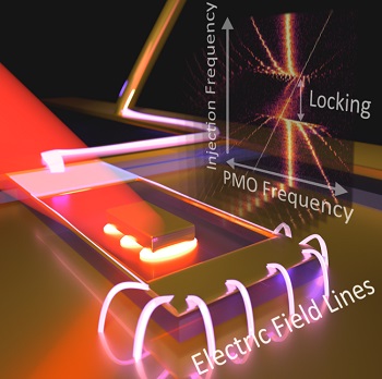
Imagine a single particle, only one-tenth the diameter of a bacterium, whose miniscule jiggles induce sustained vibrations in an entire mechanical device some 50 times larger. By taking clever advantage of the interplay between light, electrons on the surface of metals, and heat, researchers at the National Institute of Standards and Technology (NIST) have for the first time created a plasmomechanical oscillator (PMO), so named because it tightly couples plasmons—the collective oscillations of electrons at the surface of a metal nanoparticle—to the mechanical vibrations of the much larger device it’s embedded in.
The entire system, no bigger than a red blood cell, has myriad technological applications. It offers new ways to miniaturize mechanical oscillators, improve communication systems that depend on the modulation of light, dramatically amplify extremely weak mechanical and electrical signals and create exquisitely sensitive sensors for the tiny motions of nanoparticles.
The device consists of a gold nanoparticle, about 100 nanometers in diameter, embedded in a tiny cantilever—a miniature diving board—made of silicon nitride. An air gap lies sandwiched between these components and an underlying gold plate; the width of the gap is controlled by an electrostatic actuator—a thin gold film that sits atop the cantilever and bends toward the plate when a voltage is applied. The nanoparticle acts as a single plasmonic structure that has a natural, or resonant, frequency that varies with the size of the gap, just as tuning a guitar string changes the frequency at which the string reverberates.
When a light source, in this case laser light, shines on the system, it causes electrons in the resonator to oscillate, raising the temperature of the resonator. This sets the stage for a complex interchange between light, heat and mechanical vibrations in the PMO, endowing the system with several key properties.
By applying a small, direct-current voltage to the electrostatic actuator that squeezes the gap shut, Roxworthy and Aksyuk altered the optical frequency at which the resonator vibrates and the intensity of the laser light the system reflects. Such optomechanical coupling is highly desirable because it can modulate and control the flow of light on silicon chips and shape the propagation of light beams traveling in free space.
A second property relates to the heat generated by the resonator when it absorbs laser light. The heat causes the thin gold film actuator to expand. The expansion narrows the gap, decreasing the frequency at which the embedded resonator vibrates. Conversely, when the temperature decreases, the actuator contracts, widening the gap and increasing the frequency of the resonator.
Crucially, the force exerted by the actuator always kicks the cantilever in the same direction in which the cantilever is already traveling. If the incident laser light is powerful enough, these kicks cause the cantilever to undergo self-sustaining oscillations with amplitudes thousands of times larger than the oscillations of the device due to the vibration of its own atoms at room temperature.
“This is the first time that a single plasmonic resonator with dimensions smaller than visible light has been shown to produce such self-sustaining oscillations of a mechanical device,” said Roxworthy.
The team also demonstrated for the first time that if the electrostatic actuator delivers a small mechanical force to the PMO that varies in time while the system undergoes these self-sustaining oscillations, the PMO can lock onto that tiny variable signal and greatly amplify it. The researchers showed that their device can amplify a faint signal from a neighboring system even when that signal’s amplitude is as small as ten trillionths of a meter. That ability could translate into vast improvements in detecting small oscillating signals, Roxworthy says.
Share on:


Testimonial
"We’re proud to call I-Connect007 a trusted partner. Their innovative approach and industry insight made our podcast collaboration a success by connecting us with the right audience and delivering real results."
Julia McCaffrey - NCAB GroupSuggested Items
I-Connect007 Launches Advanced Electronics Packaging Digest
09/15/2025 | I-Connect007I-Connect007 is pleased to announce the launch of Advanced Electronics Packaging Digest (AEPD), a new monthly digital newsletter dedicated to one of the most critical and rapidly evolving areas of electronics manufacturing: advanced packaging at the interconnect level.
VIDEOTON EAS's Bulgarian Subsidiary Expands Into Automotive Products
09/15/2025 | VideotonVEAS Bulgaria, engaged in electronics manufacturing, has joined the ranks of VIDEOTON companies authorized to produce automotive products.
Variosystems Strengthens North American Presence with Southlake Relaunch 2025
09/15/2025 | VariosystemsVariosystems celebrated the relaunch of its U.S. facility in Southlake, Texas. After months of redesign and reorganization, the opening marked more than just the return to a modernized production site—it was a moment to reconnect with our teams, partners, and the local community.
Hanwha Aerospace to Collaborate with BAE Systems on Advanced Anti-jamming GPS for Guided Missiles
09/15/2025 | HanwhaHanwha Aerospace has signed a contract with BAE Systems to integrate next-generation, anti-jamming Global Positioning System (GPS) technology into Hanwha Aerospace’s Deep Strike Capability precision-guided weapon system.
EV Group Achieves Breakthrough in Hybrid Bonding Overlay Control for Chiplet Integration
09/12/2025 | EV GroupEV Group (EVG), a leading provider of innovative process solutions and expertise serving leading-edge and future semiconductor designs and chip integration schemes, today unveiled the EVG®40 D2W—the first dedicated die-to-wafer overlay metrology platform to deliver 100 percent die overlay measurement on 300-mm wafers at high precision and speeds needed for production environments. With up to 15X higher throughput than EVG’s industry benchmark EVG®40 NT2 system designed for hybrid wafer bonding metrology, the new EVG40 D2W enables chipmakers to verify die placement accuracy and take rapid corrective action, improving process control and yield in high-volume manufacturing (HVM).