


 Trouble in Your Tank: Implementing Direct Metallization in Advanced Substrate Packaging
 It’s Only Common Sense: Storytelling That Sells—Stop Pitching, Start Painting Pictures
 The Right Approach: Get Ready for ISO 9001 Version 6


New NIST Chip Hints at Quantum Sensors of the Future
April 12, 2018 | NISTEstimated reading time: 3 minutes
Researchers at the National Institute of Standards and Technology (NIST) have created a chip on which laser light interacts with a tiny cloud of atoms to serve as a miniature toolkit for measuring important quantities such as length with quantum precision. The design could be mass-produced with existing technology.
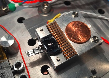
Image caption: NIST’s prototype chip for measuring important quantities such as length with quantum precision. The device works by using a laser to probe atoms to generate infrared light at a precise wavelength. The NIST chip packs a tiny cloud of atoms and structures for guiding light waves into less than 1 square centimeter. The atoms are contained in a vapor cell—the square window on top of the chip, which is surrounded by black epoxy holding a fiber-optic array. The penny is a scale reference. Credit: Hummon/NIST
As described in Optica (link is external), NIST’s prototype chip was used to generate infrared light at a wavelength of 780 nanometers, precisely enough to be used as a length reference for calibrating other instruments. The NIST chip packs the atom cloud and structures for guiding light waves into less than 1 square centimeter, about one ten-thousandth of the volume of other compact devices offering similar measurement precision.
“Compared to other devices that use chips for guiding light waves to probe atoms, our chip increases the measurement precision a hundredfold,” NIST physicist Matt Hummon said. “Our chip currently relies on a small external laser and optics table, but in future designs, we hope to put everything on the chip.”
Many devices use light to probe the quantum states of atoms in a vapor confined in a small cell. Atoms can be highly sensitive to external conditions, and therefore, make superb detectors. Devices based on light interactions with atomic vapors can measure quantities such as time, length and magnetic fields and have applications in navigation, communications, medicine and other fields. Such devices generally must be assembled by hand.
The new NIST chip transports light from the external laser through a novel waveguide and grating structure to expand the beam diameter to probe about 100 million atoms until they switch from one energy level to another. To determine the laser light frequency or wavelength that the atoms will absorb to undergo this energy transition, the system uses a photodetector to identify the laser tuning at which only about half the light passes through the vapor cell.
The demonstration used a gas of rubidium atoms, but the chip could work with a wide range of atomic and molecular vapors to generate specific frequencies across the entire visible spectrum of light and some of the infrared band. Once the laser is properly tuned, some of the original laser light can be siphoned off as output to use as a reference standard.
The NIST chip might be used, for example, to calibrate length measurement instruments. The international length standard is based on the speed of light, equivalent to the wavelength of light multiplied by its frequency.
But more importantly, the new chip shows that lasers and atomic vapor cells could potentially be mass- produced together like semiconductors, using silicon materials and traditional chip-manufacturing techniques, instead of the current manual assembly of bulky optics and blown-glass vapor cells, NIST group leader John Kitching said. This advance could apply to many NIST instruments, from atomic clocks to magnetic sensors and gas spectrometers.
The NIST chip is 14 millimeters (about 0.55 inches) long and 9 mm (about 0.35 inches) wide. The waveguides are made of silicon nitride, which can handle a wide range of light frequencies. The vapor cell is micromachined silicon with glass windows and is similar to those used in NIST’s chip-scale atomic clock and magnetometer, also developed by Kitching’s research group.
The new device measures frequency with a precision of 1 part error in 10 billion at 100 seconds, a performance verified by comparison to a separate NIST frequency comb. This performance level is very good for something so small, although full-scale lab instruments are more precise, Kitching said.
The research is part of the NIST-on-a-Chip program, aimed at creating prototypes for small, inexpensive, low-power and easily manufactured measurement tools that are quantum-based, and thus, intrinsically accurate. These tools are intended to be usable virtually anywhere, such as in industrial settings for calibration of instruments. Under this program, NIST-pioneered technologies would be manufactured and distributed by the private sector.
Share on:


Testimonial
"We’re proud to call I-Connect007 a trusted partner. Their innovative approach and industry insight made our podcast collaboration a success by connecting us with the right audience and delivering real results."
Julia McCaffrey - NCAB GroupSuggested Items
VIDEOTON EAS's Bulgarian Subsidiary Expands Into Automotive Products
09/15/2025 | VideotonVEAS Bulgaria, engaged in electronics manufacturing, has joined the ranks of VIDEOTON companies authorized to produce automotive products.
Dymax Mexico to Showcase Light-Curing Technologies at SMTA Guadalajara Expo & Tech Forum 2025
09/05/2025 | DymaxDymax, a global manufacturer of rapid light-curing materials and equipment, will participate in SMTA Guadalajara Expo & Tech Forum, taking place September 17-18, 2025, at the Guadalajara Expo Center in Guadalajara, Jalisco, Mexico.
September 2025 SMT007 Magazine: An Eye on India
09/02/2025 | I-Connect007 Editorial TeamIndia is on track to become the world’s fastest-growing major economy within the next two years, and that momentum is already reshaping its electronics manufacturing sector. Whether you work with Indian suppliers or serve Indian customers, chances are the country will become a bigger part of your supply chain in the near future.
AiM Future, Franklin Wireless Sign MOU to Jointly Develop Lightweight AI Model and High-Efficiency 1 TOPS AI SoC Chipset
09/01/2025 | BUSINESS WIREAiM Future, a leading AI semiconductor design company, has signed a Memorandum of Understanding (MOU) with Franklin Wireless Corp., a global leader in intelligent wireless solutions, to jointly develop a lightweight AI model and a high-efficiency 1 TOPS performance AI SoC chipset.
Dymax Renews Connecticut Headquarters Lease, Reinforces Long-Term Commitment to Local Community
08/08/2025 | DymaxDymax, a global manufacturer of rapid light-curing materials and equipment, is pleased to announce the renewal and extension of its corporate lease at its 318 Industrial Lane, Torrington, headquarters.