


 Trouble in Your Tank: Implementing Direct Metallization in Advanced Substrate Packaging
 It’s Only Common Sense: Storytelling That Sells—Stop Pitching, Start Painting Pictures
 The Right Approach: Get Ready for ISO 9001 Version 6


Building Crystals on a Very Hot Surface
April 16, 2018 | KAUSTEstimated reading time: 2 minutes
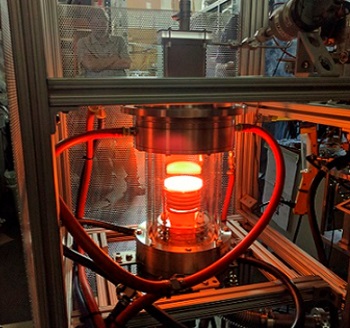
A chemical reactor that operates at extremely high temperatures is being developed by KAUST and could improve the efficiency and economy of a commonly used process in the semiconductor industry, with flow-on benefits for Saudi Arabia’s chemical industry.
The production of semiconductors relies on epitaxy: a process that creates high-quality single-crystal materials by depositing atoms on to a wafer layer by layer, controlling thickness with atomic precision.
The most common method of epitaxy is metalorganic chemical vapor deposition, or MOCVD. Pure vapors of organic molecules containing the desired atoms—for example, boron and nitrogen in the case of boron nitride—are injected into a reaction chamber. The molecules decompose on a heated wafer to leave the semiconductor’s atoms behind on the surface, which bond both to each other and the wafer to form a crystal layer.
Ph.D. student Kuang-Hui Li and a team led by Xiaohang Li at KAUST are developing an MOCVD reactor that can efficiently operate at extremely high temperatures to create high-quality boron nitride and aluminum nitride materials and devices particularly promising for flexible electronics, ultraviolet optoelectronics and power electronics.
The epitaxy of high-quality boron nitride and aluminum nitride have been a huge challenge for the conventional MOCVD process, which usually operates below 1200 degrees Celsius. Epitaxy of these materials responds best to temperatures over 1600 degrees Celsius; however, the most common resistant heaters are not reliable at these temperatures.
Although induction heaters can reach these temperatures, the heating efficiency of the conventional design is low. Because the wasted energy can overheat the gas inlet, it must be placed far away from the wafer, which is problematic for high-quality boron nitride and aluminum nitride due to particle generation and low utilization of organic molecules.
The KAUST team has developed an innovative and low-cost induction heating structure to solve these problems. “Our design can help greatly improve uniformity for up to 12-inch wafers and reduce particle generation, which is crucial for high-quality material and device fabrication,” says Kuang-Hui. “It also allows us to discover new materials”
The results show significant increase in heating efficiency and reduction in wasted energy. “This equipment research involves many disciplines and is highly complex. However, history has shown that equipment innovation is the key to scientific breakthroughs and industrial revolution,” says Xiaohang Li. “A goal of the research is to set up MOCVD manufacturing activities that can be integrated into the huge chemical industry of Saudi Arabia.”
Share on:


Testimonial
"Advertising in PCB007 Magazine has been a great way to showcase our bare board testers to the right audience. The I-Connect007 team makes the process smooth and professional. We’re proud to be featured in such a trusted publication."
Klaus Koziol - atgSuggested Items
United Electronics Corporation Unveils Revolutionary CIMS Galaxy 30 Automated Optical Inspection System
09/11/2025 | United Electronics CorporationUnited Electronics Corporation (UEC) today announced the launch of its new groundbreaking CIMS Galaxy 30 Automated Optical Inspection (AOI) machine, setting a new industry standard for precision electronics manufacturing quality control. The Galaxy 30, developed and manufactured by CIMS, represents a significant leap forward in inspection technology, delivering exceptional speed improvements and introducing cutting-edge artificial intelligence capabilities.
The Right Approach: Get Ready for ISO 9001 Version 6
09/10/2025 | Steve Williams -- Column: The Right ApproachWe are well past the normal five to seven years that a new revision of the ISO 9001 international quality standard gets released. It may be finished toward the end of 2025, with implementation starting in 2026, and there will be as many significant changes as we saw in the current 2015 version.
Machvision Leads Shift to Automated Inline Final Inspection, AOI in North America
09/10/2025 | Ralph Jacobo, all4-PCBSchweitzer Engineering Laboratories (SEL) chose Machvision inspection equipment due to its capabilities and versatility. Machvision of Taiwan offers circuit inspection, hole inspection and measurement, IC Substrate and HDI inspection, and final visual inspection solutions. The best fit for SEL was the 4.0Pro Circuit Inspection for inner and outer layers, and the AFI6 for final visual inspection of finished panels.
Federal Electronics Elevates Hermosillo Facility with Advanced Mycronic 3D AOI System
08/12/2025 | Federal ElectronicsFederal Electronics, a leader in providing advanced electronic manufacturing services, has enhanced its new production line at its Hermosillo, Mexico facility with the addition of the Mycronic MYPro i50 Automated Optical Inspection (AOI) system.
Jeh Aerospace Raises $11M to Boost Aircraft Supply Chain
08/12/2025 | I-Connect007 Editorial TeamJeh Aerospace, the high-precision aerospace and defense manufacturing startup founded by Vishal Sanghavi and Venkatesh Mudragalla, has raised $11 million in a Series A round led by Elevation Capital, with support from General Catalyst, to scale its commercial aircraft supply chain manufacturing in India, according to OEM.