


 Global PCB Connections: Rigid-flex and Flexible PCBs—The Backbone of Modern Electronics
 Flexible Thinking: The Key to a Successful Flex Circuit Design Transfer
 Happy’s Tech Talk #29: Bend-to-Install Semi-flex FR-4


Atotech Launches New Horizontal Bonding Enhancement Solution for HF Applications
April 26, 2018 | AtotechEstimated reading time: 2 minutes
BondFilm HF is Atotech’s new process for the treatment of inner layer cores. It leads to highest bonding performance in the manufacture of multilayer & HDI printed circuit boards. This innovative new process maintains the excellent performance first developed in the BondFilm product range whilst offering the lowest possible signal loss as required in high frequency applications.
Circuit design is already planning towards the low signal loss requirements of the next generation of network technology, the so called 5G. To meet these signal integrity demands the ideal would be to use a non-etching adhesion promotor system. However, whilst such systems are available in the market, they are not yet widely established. BondFilm HF bridges the gap with significantly reduced surface roughening which helps meet the signal integrity requirements whilst maintaining excellent bond strength and functional performance.
BondFilm HF
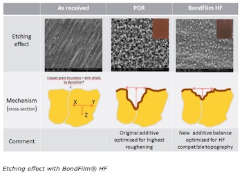
The latest development in Atotech’s BondFilm product range is BondFilm HF. Copper panels treated with BondFilm HF have the typical uniform, brown organo-metallic coating long associated with the BondFilm® process. This coating retains the excellent enhanced bonding between the inner layer and prepregs used in multilayer manufacture but with one significant difference: only minimal roughening is needed.
In previous versions of the BondFilm process development targets have been to maximize the surface roughening to give the best possible multilayer bond strength; here, the target was to provide this functional performance without compromise but with a minimal roughening of the copper traces. By producing this low roughening of the copper surface a significant reduction in signal loss in the „skin“ of the copper traces is achieved. This makes BondFilm HF more suited to high frequency applications where signal integrity is paramount.
Production trials using BondFilm HF focused on the functional properties of the multilayer boards together with electrical signal loss measurements. Data shows that panels manufactured with BondFilm HF fulfill all reliability tests considered, such as thermal stress tests and performance multiple iR reflow cycles. At the same time they significantly outperform panels made with conventional treatment processes in terms of reduced signal loss.
BondFilm HF is a simple drop in replacement for existing BondFilm process users. Its short process sequence is also compatible with most existing oxide alternative lines.
The process is already installed in a leading Chinese manufacturer and shows excellent results with first customer evaluations. Its key benefits in terms of significantly reduced signal loss gives this new process a considerable advantage for all high frequency applications.
About Atotech
Atotech is one of the world’s leading manufacturers of specialty chemicals and equipment for the printed circuit board, IC-substrate and semiconductor industries, as well as for the decorative and functional surface finishing industries. Atotech has annual sales of USD1.2 billion (2017). The company is fully committed to sustainability – we develop technologies to minimize waste and to reduce environmental impact. Atotech has its headquarters in Berlin, Germany, and employs about 4,000 people in over 40 countries. About a quarter of all staff works in one of the four locations in Germany: Berlin, Feucht, Neuruppin, and Trebur. For more information, click here.
Share on:


Testimonial
"Advertising in PCB007 Magazine has been a great way to showcase our bare board testers to the right audience. The I-Connect007 team makes the process smooth and professional. We’re proud to be featured in such a trusted publication."
Klaus Koziol - atgSuggested Items
Closing the Loop on PCB Etching Waste
09/09/2025 | Shawn Stone, IECAs the PCB industry continues its push toward greener, more cost-efficient operations, Sigma Engineering’s Mecer System offers a comprehensive solution to two of the industry’s most persistent pain points: etchant consumption and rinse water waste. Designed as a modular, fully automated platform, the Mecer System regenerates spent copper etchants—both alkaline and acidic—and simultaneously recycles rinse water, transforming a traditionally linear chemical process into a closed-loop system.
Driving Innovation: Depth Routing Processes—Achieving Unparalleled Precision in Complex PCBs
09/08/2025 | Kurt Palmer -- Column: Driving InnovationIn PCB manufacturing, the demand for increasingly complex and miniaturized designs continually pushes the boundaries of traditional fabrication methods, including depth routing. Success in these applications demands not only on robust machinery but also sophisticated control functions. PCB manufacturers rely on advanced machine features and process methodologies to meet their precise depth routing goals. Here, I’ll explore some crucial functions that empower manufacturers to master complex depth routing challenges.
Trouble in Your Tank: Minimizing Small-via Defects for High-reliability PCBs
08/27/2025 | Michael Carano -- Column: Trouble in Your TankTo quote the comedian Stephen Wright, “If at first you don’t succeed, then skydiving is not for you.” That can be the battle cry when you find that only small-diameter vias are exhibiting voids. Why are small holes more prone to voids than larger vias when processed through electroless copper? There are several reasons.
The Government Circuit: Navigating New Trade Headwinds and New Partnerships
08/25/2025 | Chris Mitchell -- Column: The Government CircuitAs global trade winds continue to howl, the electronics manufacturing industry finds itself at a critical juncture. After months of warnings, the U.S. Government has implemented a broad array of tariff increases, with fresh duties hitting copper-based products, semiconductors, and imports from many nations. On the positive side, tentative trade agreements with Europe, China, Japan, and other nations are providing at least some clarity and counterbalance.
How Good Design Enables Sustainable PCBs
08/21/2025 | Gerry Partida, Summit InterconnectSustainability has become a key focus for PCB companies seeking to reduce waste, conserve energy, and optimize resources. While many discussions on sustainability center around materials or energy-efficient processes, PCB design is an often overlooked factor that lies at the heart of manufacturing. Good design practices, especially those based on established IPC standards, play a central role in enabling sustainable PCB production. By ensuring designs are manufacturable and reliable, engineers can significantly reduce the environmental impact of their products.