


 Trouble in Your Tank: Implementing Direct Metallization in Advanced Substrate Packaging
 It’s Only Common Sense: Storytelling That Sells—Stop Pitching, Start Painting Pictures
 The Right Approach: Get Ready for ISO 9001 Version 6


Valleytronics Discovery Could Extend Limits of Moore’s Law
May 2, 2018 | Berkeley LabEstimated reading time: 3 minutes
Research appearing today in Nature Communications finds useful new information-handling potential in samples of tin(II) sulfide (SnS), a candidate “valleytronics” transistor material that might one day enable chipmakers to pack more computing power onto microchips.
The research was led by Jie Yao of the Department of Energy’s Lawrence Berkeley National Laboratory (Berkeley Lab) and Shuren Lin of UC Berkeley’s Department of Materials Science and Engineering and included scientists from Singapore and China. The research team used the unique capabilities of Berkeley Lab’s Molecular Foundry, a DOE Office of Science user facility.
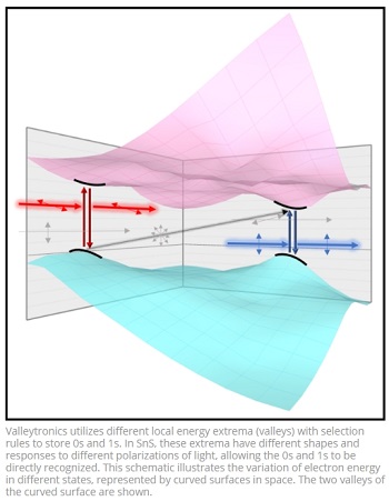
Valleytronics utilizes different local energy extrema (valleys) with selection rules to store 0s and 1s. In SnS, these extrema have different shapes and responses to different polarizations of light, allowing the 0s and 1s to be directly recognized. This schematic illustrates the variation of electron energy in different states, represented by curved surfaces in space. The two valleys of the curved surface are shown.
For several decades, improvements in conventional transistor materials have been sufficient to sustain Moore’s Law – the historical pattern of microchip manufacturers packing more transistors (and thus more information storage and handling capacity) into a given volume of silicon. Today, however, chipmakers are concerned that they might soon reach the fundamental limits of conventional materials. If they can’t continue to pack more transistors into smaller spaces, they worry that Moore’s Law would break down, preventing future circuits from becoming smaller and more powerful than their predecessors.
That’s why researchers worldwide are on the hunt for new materials that can compute in smaller spaces, primarily by taking advantage of the additional degrees of freedom that the materials offer – in other words, using a material’s unique properties to perform more computations in the same space. Spintronics, for example, is a concept for transistors that harnesses the up and down spins of electrons in materials as the on/off transistor states.
Valleytronics, another emerging approach, utilizes the highly selective response of candidate crystalline materials under specific illumination conditions to denote their on/off states – that is, using the materials’ band structures so that the information of 0s and 1s is stored in separate energy valleys of electrons, which are dependent on the crystal structures of the materials.
In this new study, the research team has shown that tin(II) sulfide (SnS) is able to absorb different polarizations of light and then selectively reemit light of different colors at different polarizations. This is useful for concurrently accessing both the usual electronic and valleytronic degrees of freedom, which would substantially increase the computing power and data storage density of circuits made with the material.
“We show a new material with distinctive energy valleys that can be directly identified and separately controlled,” said Yao. “This is important because it provides us a platform to understand how valley signatures are carried by electrons and how information can be easily stored and processed between the valleys, which are of both scientific and engineering significance.”
Lin, the first author of the paper, said the material is different from previously investigated candidate valleytronics materials because it possesses such selectivity at room temperature without additional biases apart from the excitation light source, which alleviates the previously stringent requirements in controlling the valleys. Compared to its predecessor materials, SnS is also much easier to process.
With this finding, researchers will be able to develop operational valleytronic devices, which may one day be integrated into electronic circuits. The unique coupling between light and valleys in this new material may also pave the way toward future hybrid electronic/photonic chips.
Berkeley Lab’s “Beyond Moore’s Law” initiative leverages the basic science capabilities and unique user facilities of Berkeley Lab and UC Berkeley to evaluate promising candidates for next-generation electronics and computing technologies. Its objective is to build close partnerships with industry to accelerate the time it typically takes to move from the discovery of a technology to its scale-up and commercialization.
About Lawrence Berkeley National Laboratory
Lawrence Berkeley National Laboratory addresses the world’s most urgent scientific challenges by advancing sustainable energy, protecting human health, creating new materials, and revealing the origin and fate of the universe. Founded in 1931, Berkeley Lab’s scientific expertise has been recognized with 13 Nobel Prizes. The University of California manages Berkeley Lab for the U.S. Department of Energy’s Office of Science. For more, click here.
Share on:


Testimonial
"We’re proud to call I-Connect007 a trusted partner. Their innovative approach and industry insight made our podcast collaboration a success by connecting us with the right audience and delivering real results."
Julia McCaffrey - NCAB GroupSuggested Items
Meet the Author Podcast: Martyn Gaudion Unpacks the Secrets of High-Speed PCB Design
07/16/2025 | I-Connect007In this special Meet the Author episode of the On the Line with… podcast, Nolan Johnson sits down with Martyn Gaudion, signal integrity expert, managing director of Polar Instruments, and three-time author in I-Connect007’s popular The Printed Circuit Designer’s Guide to... series.
Intervala Hosts Employee Car and Motorcycle Show, Benefit Nonprofits
08/27/2024 | IntervalaIntervala hosted an employee car and motorcycle show, aptly named the Vala-Cruise and it was a roaring success! Employees had the chance to show off their prized wheels, and it was incredible to see the variety and passion on display.
KIC Honored with IPC Recognition for 25 Years of Membership and Contributions to Electronics Manufacturing Industry
06/24/2024 | KICKIC, a renowned pioneer in thermal process and temperature measurement solutions for electronics manufacturing, is proud to announce that it has been recognized by IPC for 25 years of membership and significant contributions to electronics manufacturing.
Boeing Starliner Spacecraft Completes Successful Crewed Docking with International Space Station
06/07/2024 | BoeingNASA astronauts Barry "Butch" Wilmore and Sunita "Suni" Williams successfully docked Boeing's Starliner spacecraft to the International Space Station (ISS), about 26 hours after launching from Cape Canaveral Space Force Station.
KIC’s Miles Moreau to Present Profiling Basics and Best Practices at SMTA Wisconsin Chapter PCBA Profile Workshop
01/25/2024 | KICKIC, a renowned pioneer in thermal process and temperature measurement solutions for electronics manufacturing, announces that Miles Moreau, General Manager, will be a featured speaker at the SMTA Wisconsin Chapter In-Person PCBA Profile Workshop.